ZHCSBD3D July   2013  – August 2019 TPS63050 , TPS63051

PRODUCTION DATA.  

  1. 特性
  2. 应用
  3. 说明
    1.     Device Images
      1.      简化原理图 (WCSP)
      2.      效率与输出电流间的关系
  4. 修订历史记录
  5. Device Comparison Table
  6. Pin Configuration and Functions
    1.     Pin Functions
  7. Specifications
    1. 7.1 Absolute Maximum Ratings
    2. 7.2 ESD Ratings
    3. 7.3 Recommended Operating Conditions
    4. 7.4 Thermal Information
    5. 7.5 Electrical Characteristics
    6. 7.6 Switching Characteristics
    7. 7.7 Typical Characteristics
  8. Detailed Description
    1. 8.1 Overview
    2. 8.2 Functional Block Diagrams
    3. 8.3 Feature Description
      1. 8.3.1 Power Good
      2. 8.3.2 Overvoltage Protection
      3. 8.3.3 Undervoltage Lockout (UVLO)
      4. 8.3.4 Thermal Shutdown
      5. 8.3.5 Soft Start
      6. 8.3.6 Short Circuit Protection
    4. 8.4 Device Functional Modes
      1. 8.4.1 Control Loop Description
      2. 8.4.2 Power Save Mode Operation
      3. 8.4.3 Adjustable Current Limit
      4. 8.4.4 Device Enable
  9. Application and Implementation
    1. 9.1 Application Information
    2. 9.2 Typical Application
      1. 9.2.1 Design Requirements
      2. 9.2.2 Detailed Design Procedure
        1. 9.2.2.1 Custom Design With WEBENCH® Tools
        2. 9.2.2.2 Output Filter Design
        3. 9.2.2.3 Inductor Selection
        4. 9.2.2.4 Capacitor selection
          1. 9.2.2.4.1 Input Capacitor
          2. 9.2.2.4.2 Output Capacitor
        5. 9.2.2.5 Setting the Output Voltage
      3. 9.2.3 Application Curves
  10. 10Power Supply Recommendations
  11. 11Layout
    1. 11.1 Layout Guidelines
    2. 11.2 Layout Example (WCSP)
    3. 11.3 Layout Example (HotRod)
    4. 11.4 Thermal Considerations
  12. 12器件和文档支持
    1. 12.1 使用 WEBENCH® 工具创建定制设计
    2. 12.2 器件支持
      1. 12.2.1 第三方米6体育平台手机版_好二三四免责声明
    3. 12.3 相关链接
    4. 12.4 接收文档更新通知
    5. 12.5 社区资源
    6. 12.6 商标
    7. 12.7 静电放电警告
    8. 12.8 Glossary
  13. 13机械、封装和可订购信息

封装选项

机械数据 (封装 | 引脚)
散热焊盘机械数据 (封装 | 引脚)
订购信息

Typical Characteristics

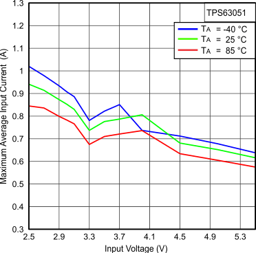
TPS63050 TPS63051 Figure3_SLVSAM8.gif
VOUT = 3.3 V
Figure 1. Maximum Average Input Current vs Input Voltage
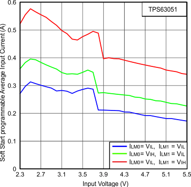
TPS63050 TPS63051 Figure5_SLVSAM8.gif
Figure 3. Programmable Average Input Current vs Input Voltage(1)
TPS63050 TPS63051 Figure4_SLVSAM8.gif
VOUT = 3.3 V
Figure 2. Minimum Average Input Current vs Input Voltage
All options only available with the DSBGA package. For VQFN package ILIM1 is internally connected to voltage level > VIH