ZHCSBD3D July   2013  – August 2019 TPS63050 , TPS63051

PRODUCTION DATA.  

  1. 特性
  2. 应用
  3. 说明
    1.     Device Images
      1.      简化原理图 (WCSP)
      2.      效率与输出电流间的关系
  4. 修订历史记录
  5. Device Comparison Table
  6. Pin Configuration and Functions
    1.     Pin Functions
  7. Specifications
    1. 7.1 Absolute Maximum Ratings
    2. 7.2 ESD Ratings
    3. 7.3 Recommended Operating Conditions
    4. 7.4 Thermal Information
    5. 7.5 Electrical Characteristics
    6. 7.6 Switching Characteristics
    7. 7.7 Typical Characteristics
  8. Detailed Description
    1. 8.1 Overview
    2. 8.2 Functional Block Diagrams
    3. 8.3 Feature Description
      1. 8.3.1 Power Good
      2. 8.3.2 Overvoltage Protection
      3. 8.3.3 Undervoltage Lockout (UVLO)
      4. 8.3.4 Thermal Shutdown
      5. 8.3.5 Soft Start
      6. 8.3.6 Short Circuit Protection
    4. 8.4 Device Functional Modes
      1. 8.4.1 Control Loop Description
      2. 8.4.2 Power Save Mode Operation
      3. 8.4.3 Adjustable Current Limit
      4. 8.4.4 Device Enable
  9. Application and Implementation
    1. 9.1 Application Information
    2. 9.2 Typical Application
      1. 9.2.1 Design Requirements
      2. 9.2.2 Detailed Design Procedure
        1. 9.2.2.1 Custom Design With WEBENCH® Tools
        2. 9.2.2.2 Output Filter Design
        3. 9.2.2.3 Inductor Selection
        4. 9.2.2.4 Capacitor selection
          1. 9.2.2.4.1 Input Capacitor
          2. 9.2.2.4.2 Output Capacitor
        5. 9.2.2.5 Setting the Output Voltage
      3. 9.2.3 Application Curves
  10. 10Power Supply Recommendations
  11. 11Layout
    1. 11.1 Layout Guidelines
    2. 11.2 Layout Example (WCSP)
    3. 11.3 Layout Example (HotRod)
    4. 11.4 Thermal Considerations
  12. 12器件和文档支持
    1. 12.1 使用 WEBENCH® 工具创建定制设计
    2. 12.2 器件支持
      1. 12.2.1 第三方米6体育平台手机版_好二三四免责声明
    3. 12.3 相关链接
    4. 12.4 接收文档更新通知
    5. 12.5 社区资源
    6. 12.6 商标
    7. 12.7 静电放电警告
    8. 12.8 Glossary
  13. 13机械、封装和可订购信息

封装选项

机械数据 (封装 | 引脚)
散热焊盘机械数据 (封装 | 引脚)
订购信息

Application Curves

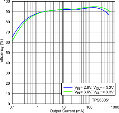
TPS63050 TPS63051 Figure13_SLVSAM8.gif
PFM/PWM = Low VOUT = 3.3 V
Figure 10. Efficiency vs Output Current
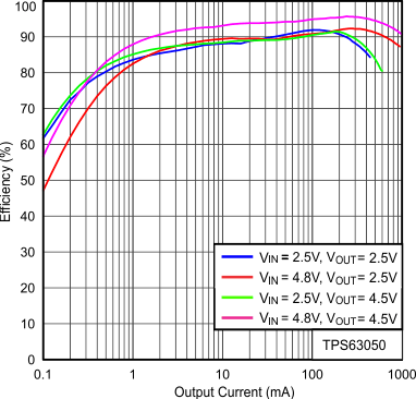
TPS63050 TPS63051 Figure15_SLVSAM8.gif
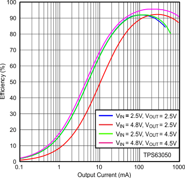
PFM/PWM = Low VOUT = 2.5 V, 4.5 V
Figure 12. Efficiency vs Output Current
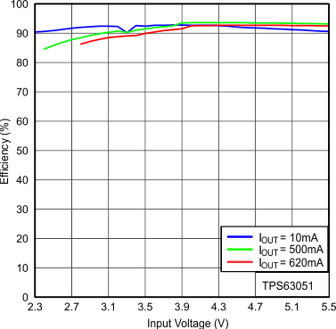
TPS63050 TPS63051 Figure17_SLVSAM8.gif
PFM/PWM = Low VOUT= 3.3 V
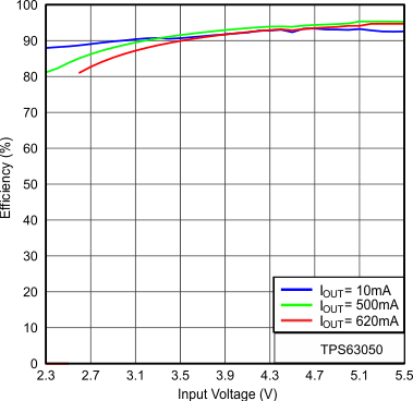
Figure 14. Efficiency vs Input Voltage
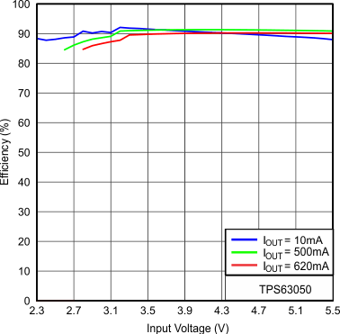
TPS63050 TPS63051 Figure19_SLVSAM8.gif
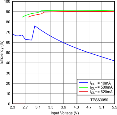
PFM/PWM = Low VOUT = 2.5 V
Figure 16. Efficiency vs Input Voltage
TPS63050 TPS63051 Figure21_SLVSAM8.gif
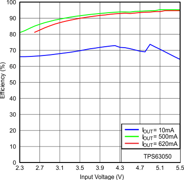
PFM/PWM = Low VOUT = 4.5 V
Figure 18. Efficiency vs Input Voltage
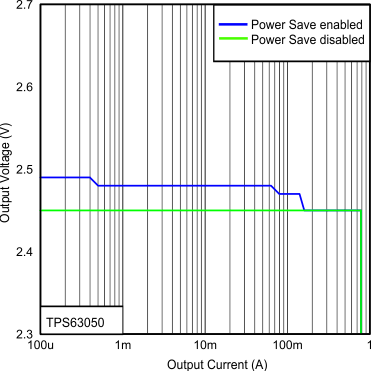
TPS63050 TPS63051 Figure23_SLVSAM8.gif
VIN = 2.5 V
Figure 20. Output Voltage vs Output Current
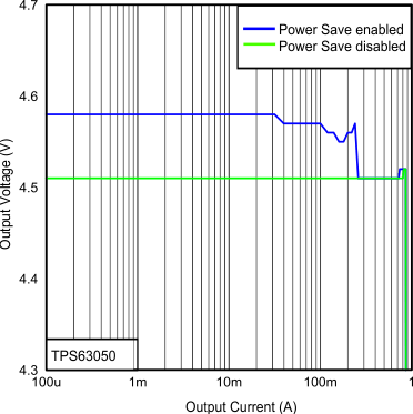
TPS63050 TPS63051 Figure25_SLVSAM8.gif
VIN = 4.5 V
Figure 22. Output Voltage vs Output Current
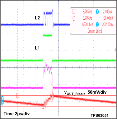
TPS63050 TPS63051 Figure27_SLVSAM8.gif
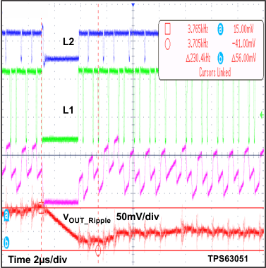
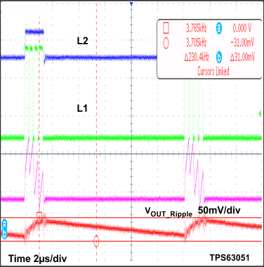
VIN = 2.8 V IOUT = 16 mA
Figure 24. Output Voltage Ripple in Boost Mode and PFM to PWM Transition
TPS63050 TPS63051 Figure29_SLVSAM8.gif
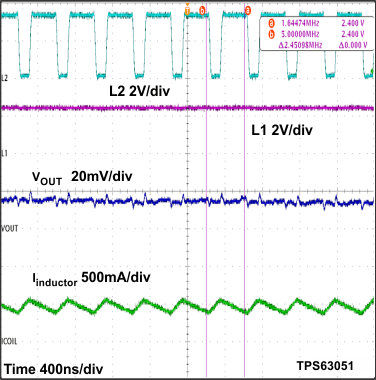
VIN = 2.5 V IOUT = 300 mA
Figure 26. Switching Waveform in Boost Mode and PWM
TPS63050 TPS63051 Figure31_SLVSAM8.gif
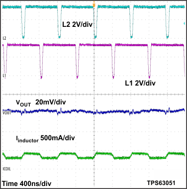
VIN = 3.4 V IOUT = 300 mA
Figure 28. Switching Waveform in Buck-Boost Mode and PWM
TPS63050 TPS63051 Figure33_SLVSAM8.gif
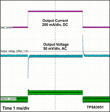
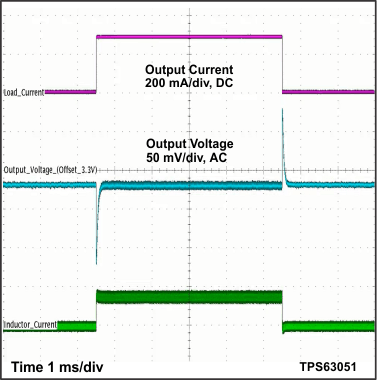
VIN = 3.6 V Load change from 0 mA to 300 mA
Figure 30. Load Transient Response
TPS63050 TPS63051 Figure35_SLVSAM8.gif
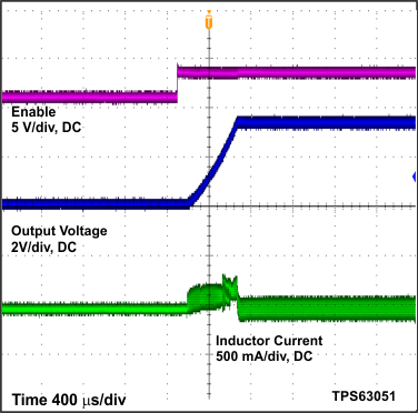
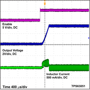
VOUT = 3.3 V VIN = 2.5 V IOUT = 0 mA
Figure 32. Start Up After Enable
TPS63050 TPS63051 Figure14_SLVSAM8.gif
PFM/PWM = High VOUT = 3.3 V
Figure 11. Efficiency vs Output Current
TPS63050 TPS63051 Figure16_SLVSAM8.gif
PFM/PWM = High VOUT = 2.5 V, 4.5 V
Figure 13. Efficiency vs Output Current
TPS63050 TPS63051 Figure18_SLVSAM8.gif
PFM/PWM = High VOUT= 3.3 V
Figure 15. Efficiency vs Input Voltage
TPS63050 TPS63051 Figure20_SLVSAM8.gif
PFM/PWM = High VOUT = 2.5 V
Figure 17. Efficiency vs Input Voltage
TPS63050 TPS63051 Figure22_SLVSAM8.gif
PFM/PWM =High VOUT= 4.5 V
Figure 19. Efficiency vs Input Voltage
TPS63050 TPS63051 Figure24_SLVSAM8.gif
VIN = 3.3 V
Figure 21. Output Voltage vs Output Current
TPS63050 TPS63051 Figure26_SLVSAM8.gif
VIN = 3.3 V IOUT = 145 mA
Figure 23. Output Voltage ripple in Buck-Boost mode and PFM to PWM transition
TPS63050 TPS63051 Figure28_SLVSAM8.gif
VIN = 4.2 V IOUT = 16 mA
Figure 25. Output Voltage Ripple in Buck Mode and PFM to PWM Transition
TPS63050 TPS63051 Figure30_SLVSAM8.gif
VIN = 4.5 V IOUT = 300 mA
Figure 27. Switching Waveform in Buck Mode and PWM
TPS63050 TPS63051 Figure32_SLVSAM8.gif
VIN = 2.8 V Load change from 0 mA to 300 mA
Figure 29. Load Transient Response
TPS63050 TPS63051 Figure34_SLVSAM8.gif
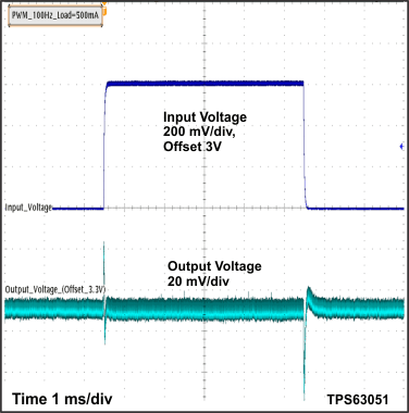
VOUT = 3.3 V IOUT = 500 mA
Figure 31. Line Transient Response
TPS63050 TPS63051 Figure36_SLVSAM8.gif
VOUT = 3.3 V VIN = 4.2 V IOUT = 0 mA
Figure 33. Start Up After Enable