ZHCS705C november 2011 – september 2020 TPS63060 , TPS63061
PRODUCTION DATA
- 1
- 1 特性
- 2 应用
- 3 说明
- 4 Revision History
- 5 Device Comparison
- 6 Pin Configuration and Functions
- 7 Specifications
- 8 Detailed Description
- 9 Application and Implementation
- 10Power Supply Recommendations
- 11Layout
- 12Device and Documentation Support
- 13Mechanical, Packaging, and Orderable Information
8.4.3 Power-Save Mode
The PS/SYNC pin can be used to select different operation modes. Power save mode improves efficiency at light load. To enable power save mode, PS/SYNC must be set low. The device enters power save mode when the average inductor current falls to a level lower than approximately 100 mA. In that situation, the converter operates with reduced switching frequency and with a minimum quiescent current to maintain high efficiency.
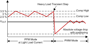
During the power save mode operation, the output voltage is monitored with a comparator by the threshold comparator low and comparator high. When the device enters power save mode, the converter stops operating and the output voltage drops. The slope of the output voltage depends on the load and the value of output capacitance. As the output voltage falls below the comparator low threshold set to 2.5% typical above the output voltage, the device ramps up the output voltage again, by starting operation using a programmed average inductor current higher than required by the current load condition. Operation can last for one or several pulses. The converter continues these pulses until the comparator high threshold, set to typically 3.5% above the nominal output voltage, is reached and the average inductor current gets lower than about 100 mA. When the load increases above the minimum forced inductor current of about 100 mA, the device automatically switches to PWM mode.
The power save mode can be disabled by programming the PS/SYNC high.
 Figure 8-4 Power-Save Mode Thresholds and Dynamic Voltage Positioning