SLVS530D SEPTEMBER 2005 – October 2015 TPS63700
PRODUCTION DATA.
- 1 Features
- 2 Applications
- 3 Description
- 4 Revision History
- 5 Pin Configuration and Functions
- 6 Specifications
- 7 Detailed Description
- 8 Application and Implementation
- 9 Power Supply Recommendations
- 10Layout
- 11Device and Documentation Support
- 12Mechanical, Packaging, and Orderable Information
8 Application and Implementation
NOTE
Information in the following applications sections is not part of the TI component specification, and TI does not warrant its accuracy or completeness. TI’s customers are responsible for determining suitability of components for their purposes. Customers should validate and test their design implementation to confirm system functionality.
8.1 Application Information
The TPS63700 DC/DC converter is intended for systems typically powered by a single-cell Li-ion or Li-polymer battery with a terminal voltage between 2.7 V up to 4.2 V. Due to the recommended input voltage going up to 5.5 V, the device is also suitable for 3-cell alkaline, NiCd,or NiMH batteries, as well as regulated supply voltages of 3.3 V or 5 V.
8.2 Typical Application
8.2.1 Design Requirements
The design of the inverter can be adapted to different output voltage and load current needs by choosing external components appropriately. The following design procedure is adequate for the whole VIN, VOUT and load current range of TPS63700.
Table 1 shows the list of components for the Application Curves.
Table 1. List of Components
| REFERENCE | DESCRIPTION |
|---|---|
| C1, C2, C3, C4, | X7R/X5R ceramic |
| C5 | 4 × 4.7 μF X7R/X5R ceramic |
| D1 | SL03/SL02 Vishay |
| L1 | –5V: TDK VLF4012 4R7, TDK SLF6025-4R7, Coilcraft LPS4018-472, |
| –12V: Sumida CDRH5D18 10 μH |
8.2.2 Detailed Design Procedure
8.2.2.1 Programming the Output Voltage: Converter
The output voltage of the TPS63700 converter can be adjusted with an external resistor divider connected to the FB pin. The reference point of the feedback divider is the reference voltage VREF with 1.213 V. The typical value of the voltage at the FB pin is 0 V. The minimum recommended output voltage at the converter is –15 V. The feedback divider current should be 10 μA. The voltage across R2 is 1.213 V. Based on those values, the recommended value for R2 should be 120 kΩ to 200 kΩ in order to set the divider current at the required value. The value of the resistor R3 can then be calculated using Equation 1, depending on the needed output voltage (VOUT).

For example, if an output voltage of –5 V is needed and a resistor of 150 kΩ has been chosen for R2, a 619-kΩ resistor is needed to program the desired output voltage.
8.2.2.1.1 Inductor Selection
An inductive converter normally requires two main passive components for storing energy during the conversion. An inductor and a storage capacitor at the output are required.
The average inductor current depends on the output load, the input voltage VIN, and the output voltage VOUT. It can be estimated with Equation 2, which shows the formula for the inverting converter.

where
- ILavg= Average inductor current
An important parameter for choosing the inductor is the desired current ripple in the inductor.
A ripple current value between 20% and 80% of the average inductor current can be considered as reasonable, depending on the application requirements. A smaller ripple reduces the losses in the inductor, as well as output voltage ripple and EMI. But in the same way, the inductor becomes larger and more expensive.
Keeping those parameters in mind, the possible inductor value can be calculated using Equation 3.

where
- ΔIL = Peak-to-peak ripple current
- f = Switching frequency
- L = Inductor value
With the known inductor current ripple, the peak inductor value can be approximated with Equation 4. The peak current through the switch and the inductor depends also on the output load, the input voltage VIN, and the output voltage VOUT. To select the right inductor, it is recommended to keep the possible peak inductor current below the current-limit threshold of the power switch. For example, the current-limit threshold of the TPS63700 switch for the inverting converter is nominally 1000 mA.

where
- ILMAX = Peak inductor current
- ΔIL = Peak-to-peak ripple current
With Equation 5, the inductor current ripple at a given inductor can be approximated.

where
- ΔIL = Peak-to-peak ripple current
- L = Inductor value
- f = Switching frequency
Care has to be taken for the possibility that load transients and losses in the circuit can lead to higher currents as estimated in Equation 4. Also, the losses caused by magnetic hysteresis losses and copper losses are a major parameter for total circuit efficiency.
The following inductor series from different suppliers have been tested with the TPS63700 converter, see Table 2.
Table 2. List of Inductors
| Output Voltage | Vendor | SUGGESTED INDUCTOR |
|---|---|---|
| –5 V | TDK | VLF4012 4.7 μH |
| SLF6025-4.7 μH | ||
| –5 V | Coilcraft | LPS4018 4.7 μH |
| LPS3015 4.7 μH | ||
| –12 V | Sumida | CDRH5D18 10 μH |
| –12 V | Coilcraft | MOS6020 10 μH |
8.2.2.2 Capacitor Selection
8.2.2.2.1 Input Capacitor
At least a 10-μF ceramic input capacitor is recommended for a good transient behavior of the regulator, and EMI behavior of the total power supply circuit.
8.2.2.2.2 Output Capacitors
One of the major parameters necessary to define the capacitance value of the output capacitor is the maximum allowed output voltage ripple of the converter. This ripple is determined by two parameters of the capacitor, the capacitance and the ESR. It is possible to calculate the minimum capacitance needed for the defined ripple, supposing that the ESR is zero, by using Equation 6 for the inverting converter output capacitor.

where
- f = Switching frequency
- ΔV = Maximum allowed ripple
- Cmin = Minimum capacitance
With a chosen ripple voltage in the range of 10 mV, a minimum capacitance of 12 μF is needed. The total ripple is larger due to the ESR of the output capacitor. This additional component of the ripple can be calculated using Equation 7 .

where
- ΔVESR = Voltage ripple caused by RESR of capacitor
- RESR = Equivalent series resistance of capacitor
An additional ripple of 2 mV is the result of using a typical ceramic capacitor with an ESR in a 10-mΩ range. The total ripple is the sum of the ripple caused by the capacitance, and the ripple caused by the ESR of the capacitor. In this example, the total ripple is 12 mV. Additional ripple is caused by load transients. When the load current increases rapidly, the output capacitor must provide the additional current until the inductor current has been increased by the control loop by setting a higher on-time at the main switch (duty cycle). The higher duty cycle results in longer inductor charging periods, but the rate of increase of the inductor current is also limited by the inductance itself. When the load current decreases rapidly, the output capacitor needs to store the excessive energy (stored in the inductor) until the regulator has decreased the inductor current by reducing the duty cycle. The recommendation is to use higher capacitance values, as the previous calculations show.
8.2.2.3 Stabilizing the Control Loop
8.2.2.3.1 Feedback Divider
To speed up the control loop, a feed-forward capacitor of 10 pF is recommended in the feedback divider, parallel to R3.
To avoid coupling noise into the control loop from the feed-forward capacitor, the feed-forward effect can be bandwidth-limited by adding series resistor R4. A value in the range of 100 kΩ is suitable. The higher the resistance, the lower the noise coupled into the control loop system.
8.2.2.3.2 Compensation Capacitor
The control loop of the converter is completely compensated internally. However the internal feed-forward system requires an external capacitor. A 4.7-nF capacitor at the COMP pin of the converter is recommended.
8.2.3 Application Curves
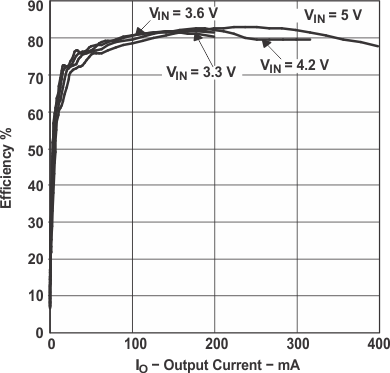 Figure 3. Efficiency vs Output Current,
VOUT –5 V
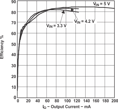 Figure 5. Efficiency vs Output Current,
VOUT –15 V
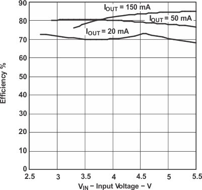 Figure 7. Efficiency vs Input Voltage,
 VOUT –12 V
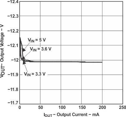 Figure 9. Output Voltage vs Output Current
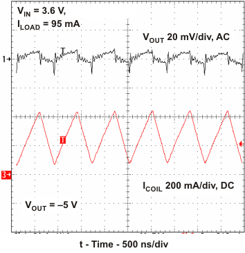 Figure 11. Output Voltage in
 Continuous Conduction Mode
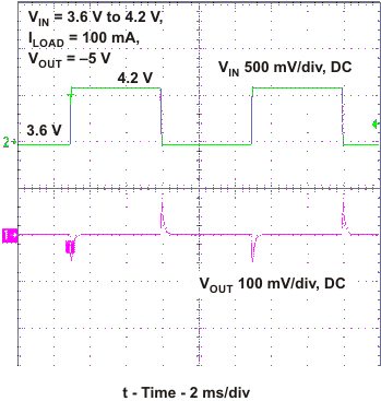 Figure 13. Line Transient Response, –5 V
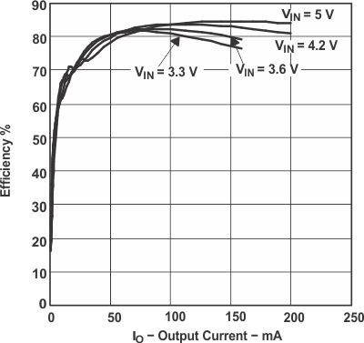 Figure 4. Efficiency vs Output Current,
VOUT –12 V
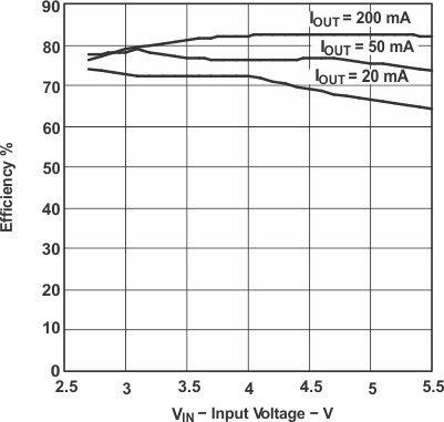 Figure 6. Efficiency vs Input Voltage,
VOUT –5 V
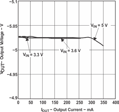 Figure 8. Output Voltage vs Output Current
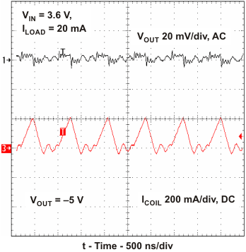 Figure 10. Output Voltage in
Discontinuous Conduction Mode
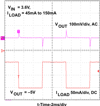 Figure 12. Load Transient Response,
 –5 V, 45 to 150 mA
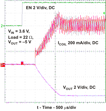 Figure 14. Start-Up After Enable, –5 V
8.3 System Example
 Figure 15. Circuit for –12-V Output
