ZHCSGR8A September 2017 – July 2018 TPS63710
PRODUCTION DATA.
- 1 特性
- 2 应用
- 3 说明
- 4 修订历史记录
- 5 Pin Configuration and Functions
- 6 Specifications
- 7 Detailed Description
- 8 Application and Implementation
- 9 Power Supply Recommendations
- 10Layout
- 11器件和文档支持
- 12机械、封装和可订购信息
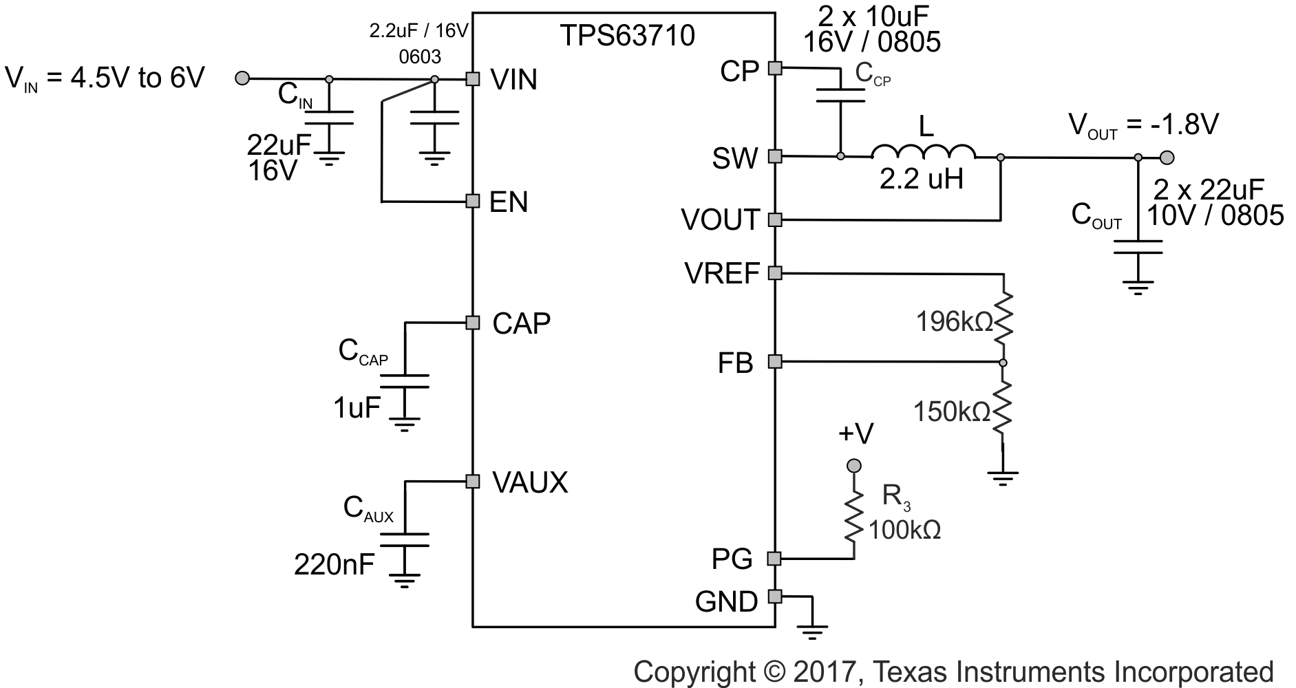
8.3.2 Typical Application for Powering the Negative Rail of an ADC or DAC
Typically, the input voltage to the inverter in applications powering the negative supply of an ADC or DAC is about 5 V. The circuit therefore was optimized for this input voltage range, because the size and amount of capacitors depends on the voltage applied to the capacitors. In order not to over-design, the input voltage range was set to the range required to set a limit for the dc bias of the capacitors. Figure 42 shows a, for an input voltage of 5-V, optimized design. The minimum input voltage to support the full output current is 4.5 V. The maximum input voltage is defined by the dc bias characteristic of the input and CCP capacitors. If a higher input voltage is required, these capacitors have to be adjusted accordingly.
 Figure 42. Typical Application for VIN ≈ 5 V