ZHCSKE6C July 2019 – February 2020 TPS63810 , TPS63811
PRODUCTION DATA.
- 1 特性
- 2 应用
- 3 说明
- 4 修订历史记录
- 5 器件比较表
- 6 Pin Configuration and Functions
- 7 Specifications
-
8 Detailed Description
- 8.1 Overview
- 8.2 Functional Block Diagram
- 8.3
Feature Description
- 8.3.1 Control Scheme
- 8.3.2 Control Scheme
- 8.3.3 Power-Save Mode Operation (PSM)
- 8.3.4 Forced-PWM Operation (FPWM)
- 8.3.5 Ramp-PWM Operation (RPWM)
- 8.3.6 Device Enable (EN)
- 8.3.7 Undervoltage Lockout (UVLO)
- 8.3.8 Soft Start
- 8.3.9 Output Voltage Control
- 8.3.10 Protection Functions
- 8.3.11 Power Good
- 8.3.12 Load Disconnect
- 8.3.13 Output Discharge
- 8.4 Device Functional Modes
- 8.5 Programming
- 8.6
Register Map
- 8.6.1
Register Description
- 8.6.1.1 Register Map
- 8.6.1.2 Register CONTROL (Slave address: 0b1110101; Register address: 0x01; Default: 0x00 or 0x20)
- 8.6.1.3 Register STATUS (Slave address: 0b1110101; Register address: 0x02; Default: 0x00)
- 8.6.1.4 Register DEVID (Slave address: 0b1110101; Register address: 0x03; Default: 0x04)
- 8.6.1.5 Register VOUT1 (Slave address: 0b1110101; Register address: 0x04; Default: 0x3C)
- 8.6.1.6 Register VOUT2 (Slave address: 0b1110101; Register address: 0x05; Default: 0x42)
- 8.6.1
Register Description
- 9 Application and Implementation
- 10Power Supply Recommendations
- 11Layout
- 12器件和文档支持
- 13机械、封装和可订购信息
8.3.2 Control Scheme
The device uses a constant off-time, peak-current-mode control scheme where an outer voltage control loop generates the demand signal for an inner current control loop. During the on-time, the inner current control loop monitors the inductor current, and when the inductor current equals the demand signal from the error amplifier, the on-time stops and the next part of the switching cycle starts.
The off-time is a function of VI and VO and the operating mode (buck, boost, or buck-boost) of the converter.
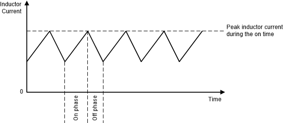 Figure 7. Peak Current Control (Buck and Boost Operation)
 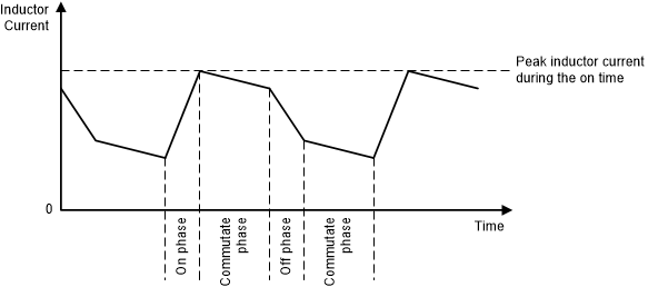 Figure 8. Peak Current Control – Buck-Boost Operation with VI < VO
 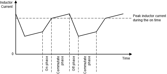 Figure 9. Peak Current Control – Buck-Boost Operation with VI > VO
 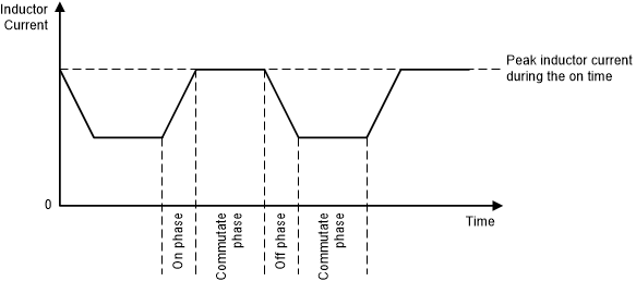 Figure 10. Peak Current Control – Buck-Boost Operation with VI = VO
 During PWM operation, current can flow in the reverse direction (from output to input). In this case, the error amplifier provides a negative peak current target. Note that the average reverse current is greater (more negative) than the peak current (see Figure 11 and Figure 12).
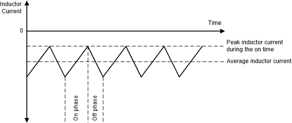 Figure 11. Reverse Peak Current Control – Buck and Boost Operation
 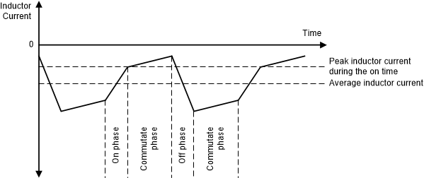 Figure 12. Reverse Peak Current Control – Buck-Boost Operation, with VI > VO