SLVS810C June 2009 – September 2015 TPS65000 , TPS650001 , TPS650003 , TPS650006 , TPS65001 , TPS650061
PRODUCTION DATA.
- 1 Features
- 2 Applications
- 3 Description
- 4 Revision History
- 5 Description (continued)
- 6 Device Options
- 7 Pin Configuration and Functions
- 8 Specifications
- 9 Detailed Description
- 10Application and Implementation
- 11Power Supply Recommendations
- 12Layout
- 13Device and Documentation Support
- 14Mechanical, Packaging, and Orderable Information
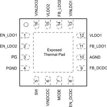
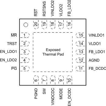
7 Pin Configuration and Functions
RTE Package
16-Pin WQFN With Exposed Thermal Pad
Top View

RUK Package
20-Pin WQFN With Exposed Thermal Pad
Top View

Pin Functions
| PIN | I/O | DESCRIPTION | ||
|---|---|---|---|---|
| NAME | 16-PIN RTE | 20-PIN RUK | ||
| AGND | 10 | 12 | — | Analog ground - Start back to PGND as close to the IC as possible. |
| EN_DCDC | 8 | 10 | I | Enable DC-DC converter |
| EN_LDO1 | 1 | 3 | I | Enable LDO1 |
| EN_LDO2 | 2 | 4 | I | Enable LDO2 |
| FB_DCDC | 9 | 11 | I | Voltage to DC-DC error amplifier |
| FB_LDO1 | 11 | 13 | I | Voltage to LDO1 error amplifier |
| FB_LDO2 | 14 | 16 | I | Voltage to LDO2 error amplifier |
| MODE | 7 | 9 | I | Selects force PWM or PWM/PFM automatic-transition mode |
| MR | — | 1 | I | Active-low input to force a reset. (1) |
| PG | 3 | 5 | O | Open-drain active low power good output. |
| PGND | 4 | 6 | — | Power ground – Connected to the thermal pad |
| RST | — | 20 | O | Open-drain active low reset output |
| RSTSNS | — | 19 | I | Voltage for RST generation |
| SW | 5 | 7 | O | Switch pin – connect inductor here |
| TRST | — | 2 | I/O | Capacitor connection for setting reset time |
| VINDCDC | 6 | 8 | I | Input voltage to DC-DC converter and all other control blocks |
| VINLDO1 | 13 | 15 | I | Input voltage to LDO1 |
| VINLDO2 | 16 | 18 | I | Input voltage to LDO2 |
| VLDO1 | 12 | 14 | O | LDO1 output voltage |
| VLDO2 | 15 | 17 | O | LDO2 output voltage |
(1) External pull up on MR is required.