SLVSAE3A August 2010 – January 2016 TPS650231
PRODUCTION DATA.
- 1 Features
- 2 Applications
- 3 Description
- 4 Revision History
- 5 Description (continued)
- 6 Pin Configuration and Functions
-
7 Specifications
- 7.1 Absolute Maximum Ratings
- 7.2 ESD Ratings
- 7.3 Recommended Operating Conditions
- 7.4 Thermal Information
- 7.5 Electrical Characteristics
- 7.6 Electrical Characteristics: Control Signals
- 7.7 Electrical Characteristics: Supply Pins VCC, VINDCDC1, VINDCDC2, VINDCDC3, VINDCDC13
- 7.8 Electrical Characteristics: Supply Pins VBACKUP, VSYSIN, VRTC, VINLDO
- 7.9 Electrical Characteristics: VDCDC1 Step-Down Converter
- 7.10 Electrical Characteristics: VDCDC2 Step-Down Converter
- 7.11 Electrical Characteristics: VDCDC3 Step-Down Converter
- 7.12 Timing Requirements
- 7.13 Typical Characteristics
-
8 Detailed Description
- 8.1 Overview
- 8.2 Functional Block Diagrams
- 8.3
Feature Description
- 8.3.1 VRTC Output and Operation With or Without Backup Battery
- 8.3.2 Step-Down Converters, VDCDC1, VDCDC2, and VDCDC3
- 8.3.3 Power Save Mode Operation
- 8.3.4 Low-Ripple Mode
- 8.3.5 Soft-Start
- 8.3.6 100% Duty Cycle Low-Dropout Operation
- 8.3.7 Active Discharge When Disabled
- 8.3.8 Power-Good Monitoring
- 8.3.9 Low-Dropout Voltage Regulators
- 8.3.10 Undervoltage Lockout
- 8.3.11 Power-Up Sequencing
- 8.3.12 System Reset + Control Signals
- 8.4 Device Functional Modes
- 8.5 Programming
- 8.6
Register Maps
- 8.6.1 VERSION Register Address: 00h (Read Only)
- 8.6.2 PGOODZ Register Address: 01h (Read Only)
- 8.6.3 MASK Register Address: 02h (Read or Write), Default Value: C0h
- 8.6.4 REG_CTRL Register Address: 03h (Read or Write), Default Value: FFh
- 8.6.5 CON_CTRL Register Address: 04h (Read or Write), Default Value: B1h
- 8.6.6 CON_CTRL2 Register Address: 05h (Read or Write), Default Value: 40h
- 8.6.7 DEFCORE Register Address: 06h (Read or Write), Default Value: 14h/1Eh
- 8.6.8 DEFSLEW Register Address: 07h (Read or Write), Default Value: 06h
- 8.6.9 LDO_CTRL Register Address: 08h (Read or Write), Default Value: Set with DEFLDO1 and DEFLDO2
- 9 Application and Implementation
- 10Power Supply Recommendations
- 11Layout
- 12Device and Documentation Support
- 13Mechanical, Packaging, and Orderable Information
封装选项
机械数据 (封装 | 引脚)
散热焊盘机械数据 (封装 | 引脚)
- RSB|40
订购信息
11 Layout
11.1 Layout Guidelines
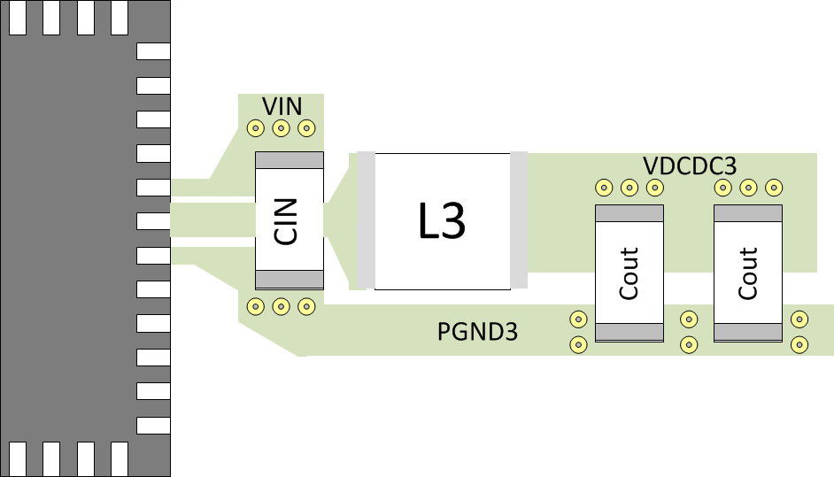
As for all switching power supplies, the layout is an important step in the design. Proper function of the device demands careful attention to PCB layout. Take care in board layout to get the specified performance. If the layout is not carefully done, the regulators may show poor line and/or load regulation, and stability issues, as well as EMI problems. It is critical to provide a low impedance ground path. Therefore, use wide and short traces for the main current paths. The input capacitors must be placed as close as possible to the IC pins as well as the inductor and output capacitor.
For TPS650231RSB, connect the PGND pins of the device to the PowerPAD land of the PCB and connect the analog ground connections (AGND) to the PGND at the PowerPAD. It is essential to provide a good thermal and electrical connection of all GND pins using multiples through to the GND-plane. Keep the common path to the AGND pins, which returns the small signal components, and the high current of the output capacitors as short as possible to avoid ground noise. The VDCDCx line must be connected right to the output capacitor and routed away from noisy components and traces (for example, the L1, L2, and L3 traces).
For TPS650231YFF, connect the PGND pins of the device and the analog ground connections (AGND) to the GND plane on the board. It is essential to provide a good thermal and electrical connection of all GND pins to the GND-plane. Keep the common path to the AGND pins, which returns the small signal components, and the high current of the output capacitors as short as possible to avoid ground noise. The VDCDCx line must be connected right to the output capacitor and routed away from noisy components and traces (for example, the L1, L2, and L3 traces).
11.2 Layout Example
 Figure 47. DC–DC Regulator Layout Example