SLVS844A September 2008 – June 2015 TPS65055
PRODUCTION DATA.
- 1 Features
- 2 Applications
- 3 Description
- 4 Revision History
- 5 Pin Configuration and Functions
- 6 Specifications
- 7 Parameter Measurement Information
- 8 Detailed Description
- 9 Application and Implementation
- 10Power Supply Recommendations
- 11Layout
- 12Device and Documentation Support
- 13Mechanical, Packaging, and Orderable Information
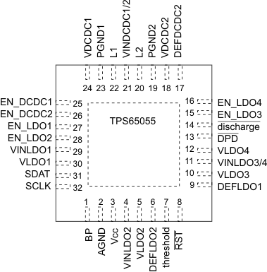
5 Pin Configuration and Functions
RSM Package
32-Pin VQFN
Top View

Pin Functions
| PIN | I/O | DESCRIPTION | |
|---|---|---|---|
| NAME | NO. | ||
| AGND | 2 | I | Analog GND, connect to PGND and PowerPAD |
| BP | 1 | I | Input for bypass capacitor for internal reference |
| DEF_DCDC2 | 17 | I | Select pin of converter 2 output voltage. High = 1 V, low = 1.2 V |
| DEFLDO1 | 9 | I | Digital input, used to set the default output voltage of LDO1 to LDO4; LSB |
| DEFLDO2 | 6 | I | Digital input, used to set the default output voltage of LDO1 to LDO4; MSB |
| discharge | 14 | O | Open-drain output driven by the signal at the threshold input |
| DPD | 13 | O | Open-drain active low output; low after UVLO event |
| EN_DCDC1 | 25 | I | Enable input for converter1, active high |
| EN_DCDC2 | 26 | I | Enable input for converter2, active high |
| EN_LDO1 | 27 | I | Enable input for LDO1. Logic high enables the LDO, logic low disables the LDO. |
| EN_LDO2 | 28 | I | Enable input for LDO2. Logic high enables the LDO, logic low disables the LDO. |
| EN_LDO3 | 15 | I | Enable input for LDO3. Logic high enables the LDO, logic low disables the LDO. |
| EN_LDO4 | 16 | I | Enable input for LDO4. Logic high enables the LDO, logic low disables the LDO. |
| L1 | 22 | O | Switch pin of converter1. Connected to inductor |
| L2 | 20 | O | Switch pin of converter 2. Connected to inductor. |
| PGND1 | 23 | I | GND for converter 1 |
| PGND2 | 19 | I | GND for converter 2 |
| RST | 8 | O | Open-drain active low output; low after UVLO event |
| SCLK | 32 | I | Clock input for the I2C compatible interface. |
| SDAT | 31 | I/O | Data line for the I2C compatible interface. |
| threshold | 7 | I | Input to comparator driving the discharge output. If the input voltage at threshold is < 0.8 V, the discharge output is actively pulled low. |
| Vcc | 3 | I | Power supply for digital and analog circuitry of DCDC1, DCDC2 and LDOs. This pin must be connected to the same voltage supply as VINDCDC1/2. |
| VDCDC1 | 24 | I | Feedback voltage sense input, connect directly to Vout1 |
| VDCDC2 | 18 | I | Feedback voltage sense input, connect directly to Vout2 |
| VINDCDC1/2 | 21 | Input voltage for VDCDC1 and VDCDC2 step-down converter. This must be connected to the same voltage supply as VCC. | |
| VINLDO1 | 29 | I | Input voltage for LDO1 |
| VINLDO2 | 4 | I | Input voltage for LDO2 |
| VINLDO3/4 | 11 | I | Input voltage for LDO3 and LDO4 |
| VLDO1 | 30 | O | Output voltage of LDO1 |
| VLDO2 | 5 | O | Output voltage of LDO2 |
| VLDO3 | 10 | O | Output voltage of LDO3 |
| VLDO4 | 12 | O | Output voltage of LDO4 |
| PowerPAD™ | – | Connect to GND | |