SLVS844A September 2008 – June 2015 TPS65055
PRODUCTION DATA.
- 1 Features
- 2 Applications
- 3 Description
- 4 Revision History
- 5 Pin Configuration and Functions
- 6 Specifications
- 7 Parameter Measurement Information
- 8 Detailed Description
- 9 Application and Implementation
- 10Power Supply Recommendations
- 11Layout
- 12Device and Documentation Support
- 13Mechanical, Packaging, and Orderable Information
6 Specifications
6.1 Absolute Maximum Ratings
over operating free-air temperature range (unless otherwise noted) (1)| MIN | MAX | UNIT | ||
|---|---|---|---|---|
| Input voltage range on all pins except A/PGND, EN_LDO1 pins with respect to AGND | –0.3 | 7 | V | |
| Input voltage range on EN_LDO1 pins with respect to AGND | –0.3 | VCC+0.5 | V | |
| Output voltage range on LDO1, LDO2, LDO3, LDO4 pins with respect to AGND | –0.3 | 4 | V | |
| Current at VINDCDC1/2, L1, PGND1, L2, PGND2 | 1800 | mA | ||
| Current at all other pins | 1000 | mA | ||
| Continuous total power dissipation | See Dissipation Ratings | |||
| TA | Operating free-air temperature | –40 | 85 | °C |
| TJ | Maximum junction temperature | 125 | °C | |
| Lead temperature 1,6 mm (1/16-inch) from case for 10 seconds | 260 | °C | ||
| Tst | Storage temperature | –65 | 150 | °C |
(1) Stresses beyond those listed under Absolute Maximum Ratings may cause permanent damage to the device. These are stress ratings only and functional operation of the device at these or any other conditions beyond those indicated under Recommended Operating Conditions is not implied. Exposure to absolute-maximum-rated conditions for extended periods may affect device reliability. This device contains circuits to protect its inputs and outputs against damage due to high static voltages or electrostatic fields. These circuits have been qualified to protect this device against electrostatic discharges; HBM according to EIA/JESD22-A114-B: 1.5 kV; and CDM according EIA/JESD22C101C: 500 V, however, it is advised that precautions should be taken to avoid application of any voltage higher than maximum-rated voltages to these high-impedance circuits. During storage or handling, the device leads should be shorted together or the device should be placed in conductive foam. In a circuit, unused inputs should always be connected to an appropriated logic voltage level, preferably either VCC or ground. Specific guidelines for handling devices of this type are contained in the publication Guidelines for Handling Electrostatic-Discharge-Sensitive (ESDS) Devices and Assemblies available from Texas Instruments.
6.2 ESD Ratings
| VALUE | UNIT | |||
|---|---|---|---|---|
| V(ESD) | Electrostatic discharge | Human body model (HBM), per ANSI/ESDA/JEDEC JS-001(1) | ±2000 | V |
| Charged device model (CDM), per JEDEC specification JESD22-C101(2) | ±1000 | |||
(1) JEDEC document JEP155 states that 500-V HBM allows safe manufacturing with a standard ESD control process.
(2) JEDEC document JEP157 states that 250-V CDM allows safe manufacturing with a standard ESD control process.
6.3 Recommended Operating Conditions
over operating free-air temperature range (unless otherwise noted)| MIN | NOM | MAX | UNIT | ||
|---|---|---|---|---|---|
| VINDCDC1/2 | Input voltage range for step-down converters | 2.5 | 4 | 6 | V |
| VDCDC1 | Output voltage range for VDCDC1 step-down converter | 0.6 | VINDCDC1 | V | |
| VDCDC2 | Output voltage range for VDCDC2 step-down converter | 0.6 | VINDCDC2 | V | |
| VINLDO1, VINLDO2, VINLDO3/4 | Input voltage range for LDOs | 1.5 | 6.5 | V | |
| VLDO1-3 | Output voltage range for LDO1 and LDO3 | 0.8 | 2.8 | V | |
| VLDO2-4 | Output voltage range for LDO2 and LDO4 | 1 | 3 | V | |
| IOUTDCDC1 | Output current at L1 | 600 | mA | ||
| L1 | Inductor at L1(1) | 1.5 | 2.2 | μH | |
| CINDCDC1/2 | Input capacitor at VINDCDC1/2(1) | 22 | μF | ||
| COUTDCDC1 | Output capacitor at VDCDC1(1) | 10 | 22 | μF | |
| IOUTDCDC2 | Output current at L2 | 600 | mA | ||
| L2 | Inductor at L2(1) | 1.5 | 2.2 | μH | |
| COUTDCDC2 | Output capacitor at VDCDC2(1) | 10 | 22 | μF | |
| CVCC | Input capacitor at VCC (1) | 1 | μF | ||
| Cin1-2 | Input capacitor at VINLDO1/2(1) | 2.2 | μF | ||
| Cin3-4 | Input capacitor at VINLDO3/4(1) | 2.2 | μF | ||
| COUT1-2 | Output capacitor at VLDO1-4(1) | 2.2 | μF | ||
| ILDO1,2 | Output current at VLDO1,2 | 400 | mA | ||
| ILDO3,4 | Output current at VLDO3,4 | 200 | mA | ||
| TA | Operating ambient temperature | –40 | 85 | °C | |
| TJ | Operating junction temperature | –40 | 125 | °C | |
| RCC | Resistor from battery voltage to Vcc used for filtering(2) | 1 | 10 | Ω | |
(1) See Application and Implementation for more details.
(2) Up to 2 mA can flow into Vcc when both converters are running in PWM, this resistor causes the UVLO threshold to be shifted accordingly.
6.4 Thermal Information
| THERMAL METRIC(1) | TPS65055 | UNIT | |
|---|---|---|---|
| RSM [VQFN] | |||
| 32 PINS | |||
| RθJA | Junction-to-ambient thermal resistance | 37.2 | °C/W |
| RθJC(top) | Junction-to-case (top) thermal resistance | 30.1 | °C/W |
| RθJB | Junction-to-board thermal resistance | 7.8 | °C/W |
| ψJT | Junction-to-top characterization parameter | 0.4 | °C/W |
| ψJB | Junction-to-board characterization parameter | 7.6 | °C/W |
| RθJC(bot) | Junction-to-case (bottom) thermal resistance | 2.4 | °C/W |
(1) For more information about traditional and new thermal metrics, see the Semiconductor and IC Package Thermal Metrics application report, SPRA953.
6.5 Electrical Characteristics
VIN = 3.6 V, EN = VIN, MODE = GND, L = 2.2 μH, COUT = 22 μF, TA = –40°C to 85°C, Typical values are at TA = 25°C (unless otherwise noted)| PARAMETER | TEST CONDITIONS | MIN | TYP | MAX | UNIT | |||
|---|---|---|---|---|---|---|---|---|
| SUPPLY CURRENT | ||||||||
| Vcc | Input voltage range | 2.5 | 6 | V | ||||
| IQ | Operating quiescent current Total current into VCC, VINDCDC1/2, VINLDO1, VINLDO2, VINLDO3/4 |
One converter, IOUT = 0 mA. PFM mode enabled; device not switching, EN_DCDC1 = VIN or EN_DCDC2 = VIN; EN_LDO1 = EN_LDO2 = EN_LDO3/4 = GND |
30 | 40 | μA | |||
| Two converters, IOUT = 0 mA, PFM mode device not switching, EN_DCDC1 = VIN and EN_DCDC2 = VIN; EN_LDO1 = EN_LDO2 = EN_LDO3/4 = GND |
40 | 55 | μA | |||||
| One converter, IOUT = 0 mA, PFM mode enabled; device not switching, EN_DCDC1 = VIN or EN_DCDC2 = VIN; EN_LDO1 = EN_LDO2 = EN_LDO3 = EN_LDO4 = VIN |
190 | 260 | μA | |||||
| IQ | Operating quiescent current into VCC | One converter, IOUT = 0 mA, Switching with no load, PWM operation EN_DCDC1 = VIN or EN_DCDC2 = VIN; EN_LDO1 = EN_LDO2 = EN_LDO3/4 = GND |
0.85 | mA | ||||
| Two converters, IOUT = 0 mA, Switching with no load, PWM operation EN_DCDC1 = VIN AND EN_DCDC2 = VIN; EN_LDO1 = EN_LDO2 = EN_LDO3/4 = GND |
1.25 | mA | ||||||
| I(SD) | Shutdown current | EN_DCDC1 = EN_DCDC2 = GND EN_LDO1 = EN_LDO2 = EN_LDO3 = EN_LDO4 = GND |
18 | 22 | μA | |||
| V(UVLO) | Undervoltage lockout threshold for DCDC converters and LDOs | Voltage at VCC | 1.8 | 2 | V | |||
| EN_DCDC1, EN_DCDC2, DEFDCDC2, DEFLDO1, DEFLDO2, EN_LDO1, EN_LDO2, EN_LDO3, EN_LDO4 | ||||||||
| VIH | High-level input voltage, SDAT, SCLK, EN_DCDC1, EN_DCDC2, DEFDCDC2, EN_LDO1, EN_LDO2, EN_LDO3, EN_LDO4 |
1.2 | VCC | V | ||||
| VIL | Low-level input voltage SDAT, SCLK, EN_DCDC1, EN_DCDC2, EN_LDO1, EN_LDO2, EN_LDO3, EN_LDO4, DEFDCDC2 |
0 | 0.4 | V | ||||
| IIN | Input bias current SDAT, SCLK, EN_DCDC1, EN_DCDC2, DEFDCDC2, DEFLDO1, DEFLDO2, EN_LDO1, EN_LDO2, EN_LDO3, EN_LDO4 |
0.01 | 1 | μA | ||||
| VIH | DEFLDO1, DEFLDO2 | VCC = 2.5 V | 1.0 | V | ||||
| VIL | DEFLDO1, DEFLDO2 | VCC = 6.5 V | 0.38 | V | ||||
| RPD | Pulldown resistor at DEFLDO1, DEFLDO2 for LOW signal | Pulled to GND | 1 | kΩ | ||||
| RPU | Pullup resistor at DEFLDO1, DEFLDO2 for HIGH signal | Pulled to VCC | 1 | kΩ | ||||
| RGNDopen | Resistance at DEFLDO1, DEFLDO2 to GND to detect open state | 10 | MΩ | |||||
| RVCCopen | Resistance at DEFLDO1, DEFLDO2 to Vcc to detect open state | 20 | MΩ | |||||
| POWER SWITCH | ||||||||
| rDS(on) | P-channel MOSFET on resistance | DCDC1, DCDC2 | VINDCDC1/2 = 3.6 V | 280 | 630 | mΩ | ||
| VINDCDC1/2 = 2.5 V | 400 | |||||||
| ILD_PMOS | P-channel leakage current | VDS = 6 V | 1 | μA | ||||
| rDS(on) | N-channel MOSFET on resistance | DCDC1, DCDC2 | VINDCDC1/2 = 3.6 V | 220 | 450 | mΩ | ||
| VINDCDC1/2 = 2.5 V | 320 | |||||||
| ILK_NMOS | N-channel leakage current | VDS = 6 V | 7 | 10 | μA | |||
| I(LIMF) | Forward current limit PMOS (high-side) and NMOS (low side) | DCDC1 | 2.5 V ≤ VIN ≤ 6 V | 0.85 | 1.0 | 1.15 | A | |
| DCDC2 | 0.85 | 1.0 | 1.15 | |||||
| TSD | Thermal shutdown | Increasing junction temperature | 150 | °C | ||||
| Thermal shutdown hysteresis | Decreasing junction temperature | 20 | °C | |||||
| OSCILLATOR | ||||||||
| fSW | Oscillator frequency | 2.025 | 2.25 | 2.475 | MHz | |||
| OUTPUT | ||||||||
| VOUT | Output voltage range | 0.8 | VIN | V | ||||
| VOUT | DC output voltage accuracy | DCDC1, DCDC2(1) | VIN = 2.5 V to 6 V, Mode = GND, PFM operation, 0 mA < IOUT < IOUTMAX |
–1.5% | 0% | 3.5% | ||
| VIN = 2.5 V to 6 V, Mode = VIN, PWM operation, 0 mA < IOUT < IOUTMAX |
–1.5% | 0% | 1.5% | |||||
| ΔVOUT | Power save mode ripple voltage(2) | IOUT = 1 mA, PFM = GND, Bandwidth = 20 MHz | 25 | mVPP | ||||
| tStart | Start-up time | Time from active EN to start switching | 170 | μs | ||||
| tRamp | VOUT Ramp up time | Time to ramp from 5% to 95% of VOUT | 750 | μs | ||||
| RDIS | Internal discharge resistor at L1, L2 | 350 | Ω | |||||
| VOL | RST, DPD, discharge output low voltage | IOL = 1 mA, Vthreshold < 0.8 V | 0.3 | V | ||||
| IOL | RST, DPD sink current | 1 | mA | |||||
| discharge sink current | 10 | mA | ||||||
| RST, DPD, discharge output leakage current | Vthreshold > 0.8 V, RST and DPD outputs turned off (internal NMOS in high impedance state) | 0.01 | 1 | μA | ||||
| Vth | Vthreshold voltage | Voltage rising | 0.78 | 0.8 | 0.82 | V | ||
| Hysteresis on threshold | Voltage decreasing | 80 | mV | |||||
| VLDO1, VLDO2, VLDO3 and VLDO4 LOW DROPOUT REGULATORS | ||||||||
| VINLDO | Input voltage range for LDO1, LDO2, LDO3, LDO4 | 1.5 | 6.5 | V | ||||
| VLDO1 | LDO1 output voltage range | 0.8 | 2.8 | V | ||||
| VLDO2 | LDO2 output voltage range | 1.2 | 3 | V | ||||
| VLDO3 | LDO3 output voltage | 0.8 | 2.8 | V | ||||
| VLDO4 | LDO4 output voltage range | 1.2 | 3 | V | ||||
| IO | Maximum output current for LDO1,LDO2 | 400 | mA | |||||
| Maximum output current for LDO3, LDO4 | 200 | |||||||
| I(SC) | LDO1 and LDO2 short-circuit current limit | VLDO1 = GND, VLDO2 = GND | 800 | mA | ||||
| LDO3 and LDO4 short-circuit current limit | VLDO3 = GND, VLDO4 = GND | 400 | mA | |||||
| Dropout voltage at LDO1 | IO = 250 mA, VINLDO = 1.8 V | 600 | mV | |||||
| Dropout voltage at LDO2 | IO = 400 mA, VINLDO = 3.3 V | 450 | mV | |||||
| Dropout voltage at LDO3, LDO4 | IO = 200 mA, VINLDO = 1.8 V | 280 | mV | |||||
| Output voltage accuracy for LDO1, LDO2, LDO3 | IO = 10 mA | –2% | 1% | |||||
| Leakage current from VINLDOx to VLDOx | LDO enabled, VINLDOx = 6.5 V; VO = 1.0 V, T = 140°C | 3 | μA | |||||
| Output voltage accuracy for LDO1, LDO2, LDO3, LDO4 | IO = 10 mA | –2% | 1% | |||||
| Line regulation for LDO1, LDO2, LDO3, LDO4 | VINLDO1,2 = VLDO1,2 + 0.5 V (minimum 2.5 V) to 6.5 V, VINLDO3,4 = VLDO3,4 + 0.5 V (minimum 2.5 V) to 6.5 V, IO = 10 mA |
–1% | 1% | |||||
| Load regulation for LDO1, LDO2, LDO3, LDO4 | IO = 0mA to 400 mA for LDO1, LDO2 IO = 0mA to 200 mA for LDO3, LDO4 |
–1% | 1% | |||||
| Regulation time for LDO1, LDO2, LDO3, LDO4 | Load change from 10% to 90% | 10 | μs | |||||
| PSRR | Power supply rejection ratio | f = 10 kHz; IO = 50 mA; VI = VO + 1 V | 70 | dB | ||||
| RDIS | Internal discharge resistor at VLDO1, VLDO2, VLDO3, VLDO4 | 350 | Ω | |||||
| TSD | Thermal shutdown | Increasing junction temperature | 140 | °C | ||||
| Thermal shutdown hysteresis | Decreasing junction temperature | 20 | °C | |||||
(1) Output voltage specification does not include tolerance of external voltage programming resistors.
(2) In power save mode, PWM operation is typically entered at IPSM = VIN/32 Ώ.
6.6 Dissipation Ratings
| PACKAGE | RθJA | TA ≤ 25°C POWER RATING |
DERATING FACTOR ABOVE TA = 25°C |
TA = 70°C POWER RATING |
TA = 85°C POWER RATING |
|---|---|---|---|---|---|
| RSM(1) | 58 K/W | 1.7 W | 17 mW/K | 0.95 W | 0.68 W |
(1) The thermal resistance junction-to-case of the RSM package is 4 K/W measured on a high K board.
6.7 Typical Characteristics
Table 1. Table Of Graphs
| FIGURE | |||
|---|---|---|---|
| η | Efficiency DCDC1 (VO = 2.1 V) | vs Load current / PWM mode | Figure 1 |
| η | Efficiency DCDC1 (VO = 2.1 V) | vs Load current / PFM mode | Figure 2 |
| η | Efficiency DCDC2 (VO = 1.575 V) | vs Load current / PWM mode | Figure 3 |
| η | Efficiency DCDC2 (VO = 1.575 V) | vs Load current / PFM mode | Figure 4 |
| η | Efficiency DCDC2 (VO = 1.2 V) | vs Load current / PWM mode | Figure 5 |
| η | Efficiency DCDC2 (VO = 1.2 V) | vs Load current / PFM mode | Figure 6 |
| Output voltage ripple in PFM mode | Scope plot | Figure 7 | |
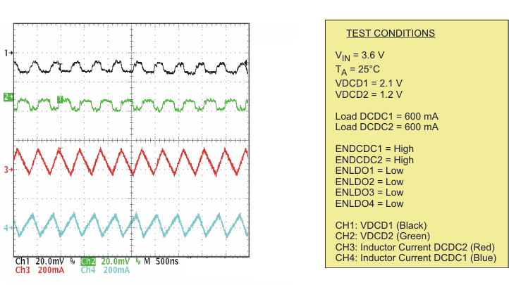
| Output voltage ripple in PWM mode | Scope plot | Figure 8 | |
| Startup timing DCDC1, DCDC2, LDO1 | Scope plot | Figure 9 | |
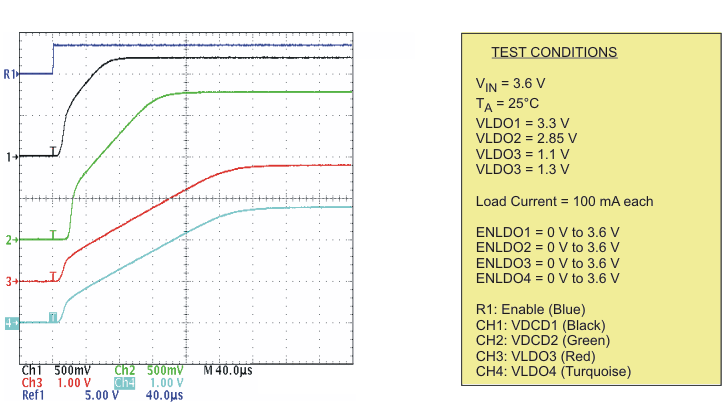
| Startup timing LDO1, LDO2, LDO3, LDO4 | Scope plot | Figure 10 | |
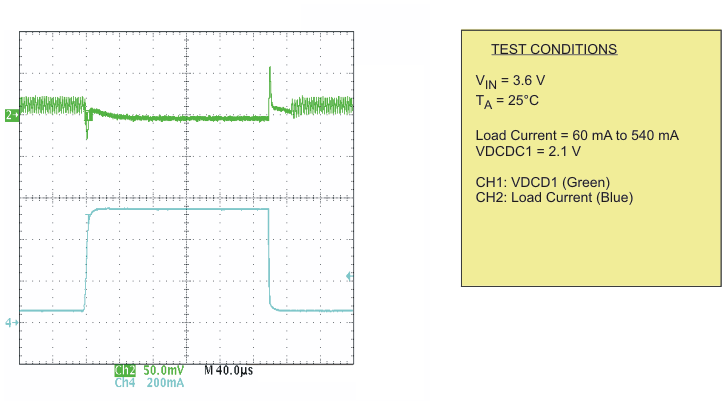
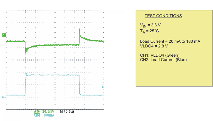
| Load transient response DCDC1; PWM | Scope plot | Figure 11 | |
| Load transient response DCDC1; PFM | Scope plot | Figure 12 | |
| Load transient response DCDC2; PWM | Scope plot | Figure 13 | |
| Load transient response DCDC2;PFM | Scope plot | Figure 14 | |
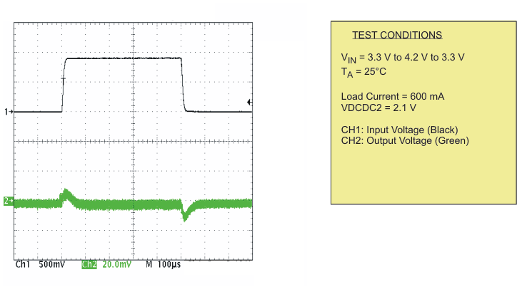
| Line transient response DCDC1 (VO = 2.1 V) | Scope plot | Figure 15 | |
| Line transient response DCDC2 (VO = 1.2 V) | Scope plot | Figure 16 | |
| Load transient response LDO1 | Scope plot | Figure 17 | |
| Load transient response LDO4 | Scope plot | Figure 18 | |
| Line transient response LDO1 | Scope plot | Figure 19 |
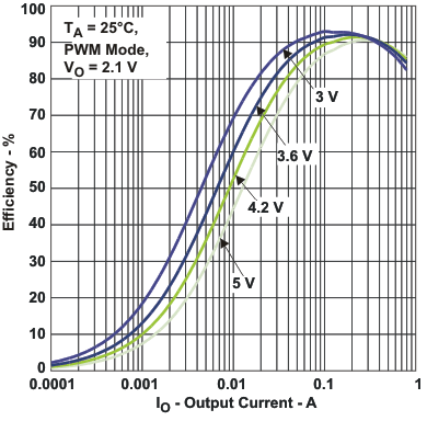 Figure 1. Efficiency DCDC1 (VO = 2.1 V) vs Load Current / PWM Mode
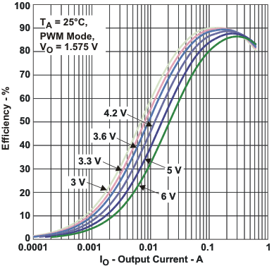 Figure 3. Efficiency DCDC2 (VO = 1.575 V) vs Load Current / PWM Mode
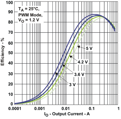 Figure 5. Efficiency DCDC2 (VO = 1.2 V) vs Load Current / PWM Mode
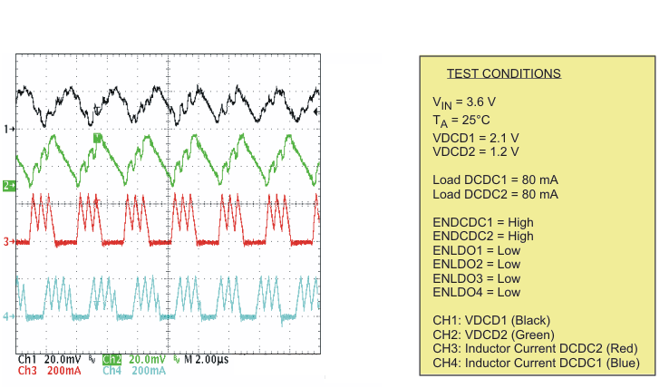
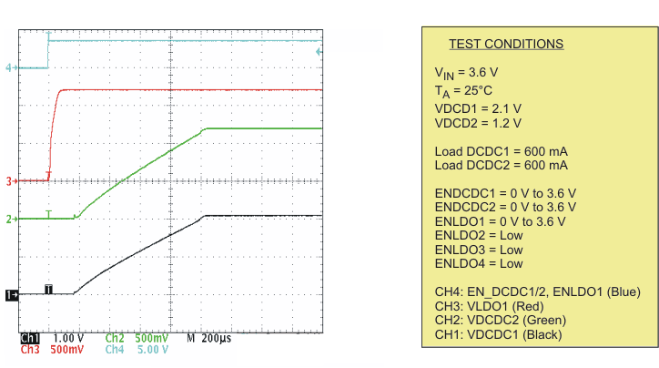
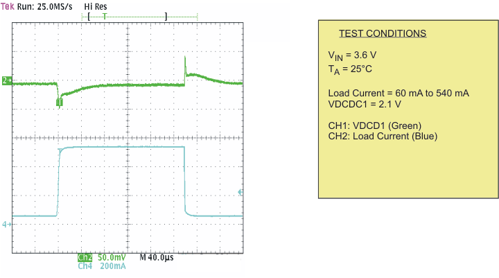
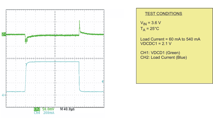
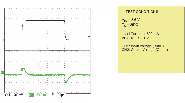
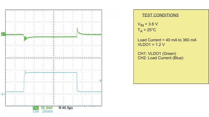
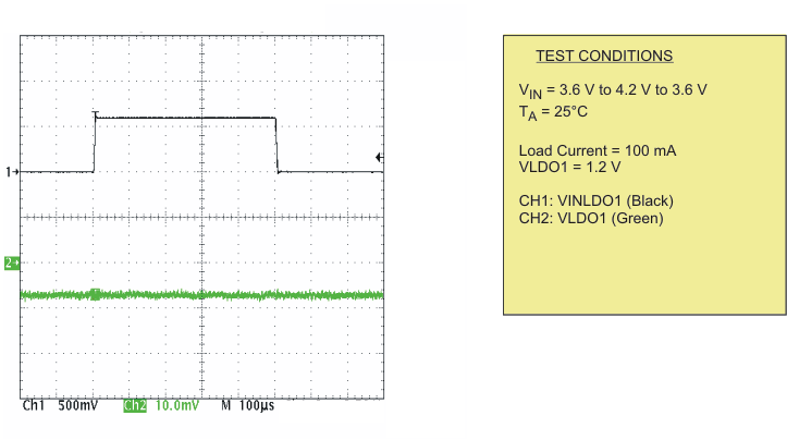
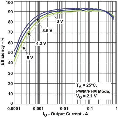 Figure 2. Efficiency DCDC1 (VO = 2.1 V) vs Load Current / PFM Mode
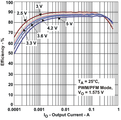 Figure 4. Efficiency DCDC2 (VO = 1.575 V) vs Load Current / PFM Mode
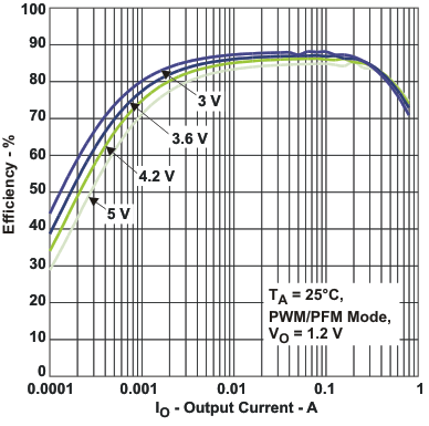 Figure 6. Efficiency DCDC2 (VO = 1.2 V) vs Load Current / PFM Mode
