SWCS128A March 2015 – December 2015
PRODUCTION DATA.
- 1 Device Overview
- 2 Revision History
- 3 Pin Configuration and Functions
-
4 Specifications
- 4.1 Absolute Maximum Ratings
- 4.2 ESD Ratings
- 4.3 Recommended Operating Conditions
- 4.4 Thermal Information
- 4.5 Electrical Characteristics: Total Current Consumption
- 4.6 Electrical Characteristics: Reference and Monitoring System
- 4.7 Electrical Characteristics: Buck Controllers
- 4.8 Electrical Characteristics: Synchronous Buck Converters
- 4.9 Electrical Characteristics: LDOs
- 4.10 Electrical Characteristics: Load Switches
- 4.11 Digital Signals: I2C Interface
- 4.12 Digital Input Signals (CTLx)
- 4.13 Digital Output Signals (IRQB, GPOx)
- 4.14 Timing Requirements
- 4.15 Switching Characteristics
- 4.16 Typical Characteristics
-
5 Detailed Description
- 5.1 Overview
- 5.2 Functional Block Diagram
- 5.3 SMPS Voltage Regulators
- 5.4 LDOs and Load Switches
- 5.5 Power Goods (PGOOD or PG) and GPOs
- 5.6 Power Sequencing and VR Control
- 5.7 Device Functional Modes
- 5.8 I2C Interface
- 5.9
Register Maps
- 5.9.1 Register Map Summary
- 5.9.2 DEVICEID: PMIC Device and Revision ID Register (offset = 1h) [reset = OTP-Programmable]
- 5.9.3 IRQ: PMIC Interrupt Register (offset = 2h) [reset = 0000 0000]
- 5.9.4 IRQ_MASK: PMIC Interrupt Mask Register (offset = 3h) [reset = 1111 1111]
- 5.9.5 PMICSTAT: PMIC Status Register (offset = 4h) [reset = 0000 0000]
- 5.9.6 SHUTDNSRC: PMIC Shut-Down Event Register (offset = 5h) [reset = 0000 0000]
- 5.9.7 BUCK1CTRL: BUCK1 Control Register (offset = 20h) [reset = OTP-Programmable]
- 5.9.8 BUCK2CTRL: BUCK2 Control Register (offset = 21h) [reset = OTP-Programmable]
- 5.9.9 BUCK3DECAY: BUCK3 Decay Control Register (offset = 22h) [reset = OTP-Programmable]
- 5.9.10 BUCK3VID: BUCK3 VID Register (offset = 23h) [reset = OTP-Programmable]
- 5.9.11 BUCK3SLPCTRL: BUCK3 Sleep Control VID Register (offset = 24h) [reset = OTP-Programmable]
- 5.9.12 BUCK4CTRL: BUCK4 Control Register (offset = 25h) [reset = OTP-Programmable]
- 5.9.13 BUCK5CTRL: BUCK5 Control Register (offset = 26h) [reset = OTP-Programmable]
- 5.9.14 BUCK6CTRL: BUCK6 Control Register (offset = 27h) [reset = OTP-Programmable]
- 5.9.15 LDOA2CTRL: LDOA2 Control Register (offset = 28h) [reset = OTP-Programmable]
- 5.9.16 LDOA3CTRL: LDOA3 Control Register (offset = 29h) [reset = OTP-Programmable]
- 5.9.17 DISCHCTRL1: Discharge Control1 Register (offset = 40h) [reset = OTP-Programmable]
- 5.9.18 DISCHCTRL2: Discharge Control2 Register (offset = 41h) [reset = OTP-Programmable]
- 5.9.19 DISCHCTRL3: Discharge Control3 Register (offset = 42h) [reset = OTP-Programmable]
- 5.9.20 PG_DELAY1: Power Good Delay1 Register (offset = 43h) [reset = OTP-Programmable]
- 5.9.21 FORCESHUTDN: Force Emergency Shutdown Control Register (offset = 91h) [reset = 0000 0000]
- 5.9.22 BUCK1SLPCTRL: BUCK1 Sleep Control Register (offset = 92h) [reset = OTP-Programmable]
- 5.9.23 BUCK2SLPCTRL: BUCK2 Sleep Control Register (offset = 93h) [reset = OTP-Programmable]
- 5.9.24 BUCK4VID: BUCK4 VID Register (offset = 94h) [reset = OTP-Programmable]
- 5.9.25 BUCK4SLPVID: BUCK4 Sleep VID Register (offset = 95h) [reset = OTP-Programmable]
- 5.9.26 BUCK5VID: BUCK5 VID Register (offset = 96h) [reset = OTP-Programmable]
- 5.9.27 BUCK5SLPVID: BUCK5 Sleep VID Register (offset = 97h) [reset = OTP-Programmable]
- 5.9.28 BUCK6VID: BUCK6 VID Register (offset = 98h) [reset = OTP-Programmable]
- 5.9.29 BUCK6SLPVID: BUCK6 Sleep VID Register (offset = 99h) [reset = OTP-Programmable]
- 5.9.30 LDOA2VID: LDOA2 VID Register (offset = 9Ah) [reset = OTP-Programmable]
- 5.9.31 LDOA3VID: LDOA3 VID Register (offset = 9Bh) [reset = OTP-Programmable]
- 5.9.32 BUCK123CTRL: BUCK1-3 Control Register (offset = 9Ch) [reset = OTP-Programmable]
- 5.9.33 PG_DELAY2: Power Good Delay2 Register (offset = 9Dh) [reset = OTP-Programmable]
- 5.9.34 SWVTT_DIS: SWVTT Disable Register (offset = 9Fh) [reset = OTP-Programmable]
- 5.9.35 I2C_RAIL_EN1: VR Pin Enable Override1 Register (offset = A0h) [reset = OTP-Programmable]
- 5.9.36 I2C_RAIL_EN2/GPOCTRL: VR Pin Enable Override2/GPO Control Register (offset = A1h) [reset = OTP-Programmable]
- 5.9.37 PWR_FAULT_MASK1: VR Power Fault Mask1 Register (offset = A2h) [reset = OTP-Programmable]
- 5.9.38 PWR_FAULT_MASK2: VR Power Fault Mask2 Register (offset = A3h) [reset = OTP-Programmable]
- 5.9.39 GPO1PG_CTRL1: GPO1 PG Control1 Register (offset = A4h) [reset = OTP-Programmable]
- 5.9.40 GPO1PG_CTRL2: GPO1 PG Control2 Register (offset = A5h) [reset = OTP-Programmable]
- 5.9.41 GPO4PG_CTRL1: GPO4 PG Control1 Register (offset = A6h) [reset = OTP-Programmable]
- 5.9.42 GPO4PG_CTRL2: GPO4 PG Control2 Register (offset = A7h) [reset = OTP-Programmable]
- 5.9.43 GPO2PG_CTRL1: GPO2 PG Control1 Register (offset = A8h) [reset = OTP-Programmable]
- 5.9.44 GPO2PG_CTRL2: GPO2 PG Control2 Register (offset = A9h) [reset = OTP-Programmable]
- 5.9.45 GPO3PG_CTRL1: GPO3 PG Control1 Register (offset = AAh) [reset = OTP-Programmable]
- 5.9.46 GPO3PG_CTRL2: GPO3 PG Control2 Register (offset = ABh) [reset = OTP-Programmable]
- 5.9.47 MISCSYSPG Register (offset = ACh) [reset = OTP-Programmable]
- 5.9.48 LDOA1CTRL: LDOA1 Control Register (offset = AEh) [reset = OTP-Programmable]
- 5.9.49 PG_STATUS1: Power Good Status1 Register (offset = B0h) [reset = 0000 0000]
- 5.9.50 PG_STATUS2: Power Good Status2 Register (offset = B1h) [reset = 0000 0000]
- 5.9.51 PWR_FAULT_STATUS1: Power Fault Status1 Register (offset = B2h) [reset = 0000 0000]
- 5.9.52 PWR_FAULT_STATUS2: Power Fault Status2 Register (offset = B3h) [reset = 0000 0000]
- 5.9.53 TEMPCRIT: Temperature Fault Status Register (offset = B4h) [reset = 0000 0000]
- 5.9.54 TEMPHOT: Temperature Hot Status Register (offset = B5h) [reset = 0000 0000]
- 5.9.55 OC_STATUS: Overcurrent Fault Status Register (offset = B6h) [reset = 0000 0000]
- 6 Application and Implementation
- 7 Power Supply Coupling and Bulk Capacitors
- 8 Layout
- 9 Device and Documentation Support
- 10Mechanical, Packaging, and Orderable Information
6 Application and Implementation
NOTE
Information in the following applications sections is not part of the TI component specification, and TI does not warrant its accuracy or completeness. TI’s customers are responsible for determining suitability of components for their purposes. Customers should validate and test their design implementation to confirm system functionality.
6.1 Application Information
6.1.1 Typical Application
For a detailed description about application usage, refer to the TPS65086x Design Guide (SLVUAJ9) and to the TPS65086x Schematic and Layout Checklist (SLVA734). The TPS650860 can be used in several different applications from computing, industrial interfacing and much more. This section describes the general application information and provides a more detailed description on the TPS650860 device that powers a generic multicore-processor application. An example system block diagram for the device powering an SoC and the rest of platform is shown in Figure 6-1. The functional block diagram from Figure 5-1 outlines the typical external components necessary for proper device functionality.
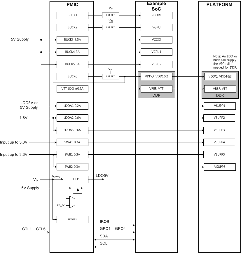 Figure 6-1 Typical Application Example
6.1.1.1 Design Requirements
The TPS650860 requires decoupling caps on the supply pins. Follow the values for recommended capacitance on these supplies given in the Specifications section. The controllers, converter, LDOs, and some other features can be adjusted to meet specific application needs. Section 6.1.1.2 describes how to design and adjust the external components to achieve desired performance.
6.1.1.2 Detailed Design Procedure
6.1.1.2.1 Controller Design Procedure
Designing the controller can be broken down into the following steps:
- Design the output filter
- Select the FETs
- Select the bootstrap capacitor
- Select the input capacitors
- Set the current limits
Controllers BUCK1, BUCK2, and BUCK6 require a 5-V supply and capacitors at their corresponding DRV5V_x_x pins. For most applications, the DRV5V_x_x input must come from the LDO5P0 pin to ensure uninterrupted supply voltage; a 2.2-µF, X5R, 20%, 10-V, or similar capacitor must be used for decoupling.
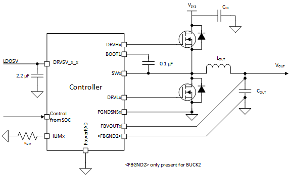 Figure 6-2 Controller Diagram
6.1.1.2.1.1 Selecting the Inductor
Placement of an inductor is required between the external FETs and the output capacitors. Together, the inductor and output capacitors make the double-pole that contributes to stability. In addition, the inductor is directly responsible for the output ripple, efficiency, and transient performance. As the inductance used increases, the ripple current decreases, which typically results in an increased efficiency. However, with an increase in inductance used, the transient performance decreases. Finally, the inductor selected must be rated for appropriate saturation current, core losses, and DC resistance (DCR).
Equation 1 shows the calculation for the recommended inductance for the controller.

where
- VOUT is the typical output voltage
- VIN is the typical input voltage
- fSW is the typical switching frequency
- IoutMAX is the maximum load current
- KIND is the ratio of ILripple to the Iout(max). For this application, TI recommends that KIND is set to a value from 0.2 to 0.4.
With the chosen inductance value, the peak current for the inductor in steady state operation, IL(max), can be calculated using Equation 2. The rated saturation current of the inductor must be higher than the IL(max) current.

Following the previous equations, the preferred inductor selected for the controllers are listed Table 6-1.
Table 6-1 Recommended Inductors
| MANUFACTURER | PART NUMBER | VALUE | SIZE | HEIGHT |
|---|---|---|---|---|
| Cyntec | PIME031B | 0.47 µH–1 µH | 3.3 mm × 3.7 mm | 1.2 mm |
| Cyntec | PIMB041B | 0.33 µH–2.2 µH | 4.45 mm × 4.75 mm | 1.2 mm |
| Cyntec | PIMB051B | 1 µH–3.3 µH | 5.4 mm × 5.75 mm | 1.2 mm |
| Cyntec | PIME051E | 0.33 µH–4.7 µH | 5.4 mm × 5.75 mm | 1.5 mm |
| Cyntec | PIMB051H | 0.47 µH–4.7 µH | 5.4 mm × 5.75 mm | 1.8 mm |
| Cyntec | PIME061B | 0.56 µH–3.3 µH | 6.8 mm × 7.3 mm | 1.2 mm |
| Cyntec | PIME061E | 0.33 µH–4.7 µH | 6.8 mm × 7.3 mm | 1.5 mm |
| Cyntec | PIMB061H | 0.1 µH–4.7 µH | 6.8 mm × 7.3 mm | 1.8 mm |
| Cyntec | PIMB062D | 0.1 µH–6.8 µH | 6.8 mm × 7.3 mm | 2.4 mm |
6.1.1.2.1.2 Selecting the Output Capacitors
TI recommends using ceramic capacitors with low ESR values to provide the lowest output voltage ripple. The output capacitor requires an X7R or an X5R dielectric. Y5V and Z5U dielectric capacitors, aside from their wide variation in capacitance over temperature, become resistive at high frequencies.
At light load currents, the controller operates in PFM mode, and the output voltage ripple is dependent on the output-capacitor value and the PFM peak inductor current. Higher output-capacitor values minimize the voltage ripple in PFM mode. To achieve specified regulation performance and low output voltage ripple, the DC-bias characteristic of ceramic capacitors must be considered. The effective capacitance of ceramic capacitors drops with increasing DC bias voltage.
TI recommends the use of small ceramic capacitors placed between the inductor and load with many vias to the PGND plane for the output capacitors of the BUCK controllers. This solution typically provides the smallest and lowest cost solution available for DCAP2 controllers.
The selection of the output capacitor is typically driven by the output transient response. Equation 3 provides a rough estimate of the minimum required capacitance to ensure proper transient response. Because the transient response is significantly affected by the board layout, some experimentation is expected in order to confirm that values derived in this section are applicable to any particular use case. Equation 3 is not meant to be an absolute requirement, but rather a rough starting point. Alternatively, some known combination values from which to begin are provided in Table 6-2.

where
- ITRAN(max) is the maximum load current step
- L is the chosen inductance
- VOUT is the minimum programmed output voltage
- VIN is the maximum input voltage
- VOVER is the maximum allowable overshoot from programmed voltage
In cases where the transient current change is very low, the DC stability may become important. Equation 4 approximates the amount of capacitance necessary to maintain DC stability. Again, this is provided as a starting point; actual values will vary on a board-to-board case.

where
- VOUT is the maximum programmed output voltage
- 50 µs is based on internal ramp setup
- VIN is the minimum input voltage
- fSW is the typical switching frequency
- L is the chosen inductance
It is necessary to choose the maximum valuable between Equation 3 and Equation 4.
Table 6-2 Known LC Combinations
| ITRAN(max) (A) | L (µH) | VOUT (V) | VOVER (V) | COUT(µF) |
|---|---|---|---|---|
| 3.5 | 0.47 | 1 | 0.05 | 220 |
| 4 | 0.47 | 1 | 0.05 | 440 |
| 5 | 0.47 | 1.35 | 0.068 | 440 |
| 8 | 0.33 | 1 | 0.06 | 640 |
| 20 | 0.22 | 1 | 0.16 | 550 |
6.1.1.2.1.3 Selecting the FETs
This controller is designed to drive two NMOS FETs. Typically, lower RDSON values are better for improving the overall efficiency of the controller, however higher gate charge thresholds will result in lower efficiency so the two need to be balanced for optimal performance. As the RDSON for the low-side FET decreases, the minimum current limit increases; therefore, ensure selection of the appropriate values for the FETs, inductor, output capacitors, and current limit resistor. The Texas Instruments' CSD87331Q3D, CSD87381P and CSD87588N devices are recommended for the controllers, depending on the required maximum current.
6.1.1.2.1.4 Bootstrap Capacitor
To ensure the internal high-side gate drivers are supplied with a stable low-noise supply voltage, a capacitor must be connected between the SWx pins and the respective BOOTx pins. TI recommends placing ceramic capacitors with the value of 0.1 µF for the controllers. During testing, a 0.1-µF, size 0402, 10-V capacitor is used for the controllers.
TI recommends reserving a small resistor in series with the bootstrap capacitor in case the turnon and turnoff of the FETs must be slowed to reduce voltage ringing on the switch node, which is a common practice for controller design.
6.1.1.2.1.5 Setting the Current Limit
The current-limiting resistor value must be chosen based on Equation 1.
6.1.1.2.1.6 Selecting the Input Capacitors
Due to the nature of the switching controller with a pulsating input current, a low ESR input capacitor is required for best input-voltage filtering and also for minimizing the interference with other circuits caused by high input-voltage spikes. For the controller, a typical 2.2-µF capacitor can be used for the DRV5V_x_x pin to handle the transients on the driver. For the FET input, 10 µF of input capacitance (after derating) is recommended for most applications. To achieve the low ESR requirement, a ceramic capacitor is recommended. However, the voltage rating and DC-bias characteristic of ceramic capacitors must be considered. For better input-voltage filtering, the input capacitor can be increased without any limit.
NOTE
Use the correct value for the ceramic capacitor capacitance after derating to achieve the recommended input capacitance.
TI recommends placing a ceramic capacitor as close as possible to the FET across the respective VSYS and PGND pins of the FETs. The preferred capacitors for the controllers are two Murata GRM21BR61E226ME44: 22-µF, 0805, 25-V, ±20%, or similar capacitors.
6.1.1.2.2 Converter Design Procedure
Designing the converter has only two steps: design the output filter and select the input capacitors.
The converter must be supplied by a 5-V source. Figure 6-3 shows a diagram of the converter.
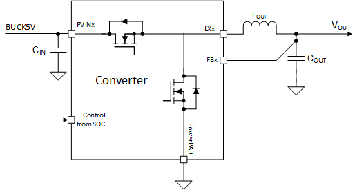 Figure 6-3 Converter Diagram
6.1.1.2.2.1 Selecting the Inductor
It is required that an inductor be placed between the external FETs and the output capacitors. Together, the inductor and output capacitors form a double pole in the control loop that contributes to stability. In addition, the inductor is directly responsible for the output ripple, efficiency, and transient performance. As the inductance used increases, the ripple current decreases, which typically results in an increase in efficiency. However, with an increase in inductance used, the transient performance decreases. Finally, the inductor selected must be rated for appropriate saturation current, core losses, and DC resistance (DCR).
NOTE
Internal parameters for the converters are optimized for a 0.47 µH inductor, however it is possible to use other inductor values as long as they are chosen carefully and thoroughly tested.
Equation 5 shows the calculation for the recommended inductance for the converter.

where
- VOUT is the typical output voltage
- VIN is the typical input voltage
- fSW is the typical switching frequency
- IoutMAX is the maximum load current
- KIND is the ratio of ILripple to the Iout(max). For this application, TI recommends that KIND is set to a value from 0.2 to 0.4.
With the chosen inductance value and the peak current for the inductor in steady state operation, IL(MAX) can be calculated using Equation 6. The rated saturation current of the inductor must be higher than the IL(MAX) current.

Following these equations, the preferred inductor selected for the converters is listed in Table 6-3.
Table 6-3 Recommended Inductors
| MANUFACTURER | PART NUMBER | VALUE | SIZE | HEIGHT |
|---|---|---|---|---|
| Cyntec | PIFE32251B-R47MS | 0.47 µH | 3.2 mm × 2.5 mm | 1.2 mm |
6.1.1.2.2.2 Selecting the Output Capacitors
Ceramic capacitors with low ESR values are recommended because they provide the lowest output voltage ripple. The output capacitor requires either an X7R or X5R rating. Y5V and Z5U capacitors, aside from the wide variation in capacitance over temperature, become resistive at high frequencies.
At light load currents, the converter operates in PFM mode and the output voltage ripple is dependent on the output-capacitor value and the PFM peak inductor current. Higher output-capacitor values minimize the voltage ripple in PFM mode. To achieve specified regulation performance and low output voltage ripple, the DC-bias characteristic of ceramic capacitors must be considered. The effective capacitance of ceramic capacitors drops with increasing DC-bias voltage.
For the output capacitors of the BUCK converters, TI recommends placing small ceramic capacitors between the inductor and load with many vias to the PGND plane. This solution typically provides the smallest and lowest-cost solution available for DCAP2 controllers.
The output capacitance must equal or exceed the minimum capacitance listed for BUCK3, BUCK4, and BUCK5 (assuming quality layout techniques are followed).
6.1.1.2.2.3 Selecting the Input Capacitors
Due to the nature of the switching converter with a pulsating input current, a low ESR input capacitor is required for best input-voltage filtering and for minimizing the interference with other circuits caused by high input-voltage spikes. For the PVINx pin, 2.5 µF of input capacitance (after derating) is required for most applications. A ceramic capacitor is recommended to achieve the low ESR requirement. However, the voltage rating and DC-bias characteristic of ceramic capacitors must be considered. The input capacitor can be increased without any limit for better input-voltage filtering.
NOTE
Use the correct value for the ceramic capacitor capacitance after derating to achieve the recommended input capacitance.
The preferred capacitor for the converters is one Samsung CL05A106MP5NUNC: 10-µF, 0402, 10-V, ±20%, or similar capacitor.
6.1.1.2.3 LDO Design Procedure
The VTT LDO must handle the fast load transients from the DDR memory for termination. Therefore, it is recommended to use ceramic capacitors to maintain a high amount of capacitance with low ESR on the VTT LDO outputs and inputs. The preferred output capacitors for the VTT LDO are the GRM188R60J226MEA0 from Murata (22 µF, 0603, 6.3 V, ±20%, or similar capacitors). The preferred input capacitor for the VTT LDO is the CL05A106MP5NUNC from Samsung (10-µF, 0402, 10-V, ±20%, or similar capacitor).
The remaining LDOs must have input and output capacitors chosen based on the values in Section 4.9.
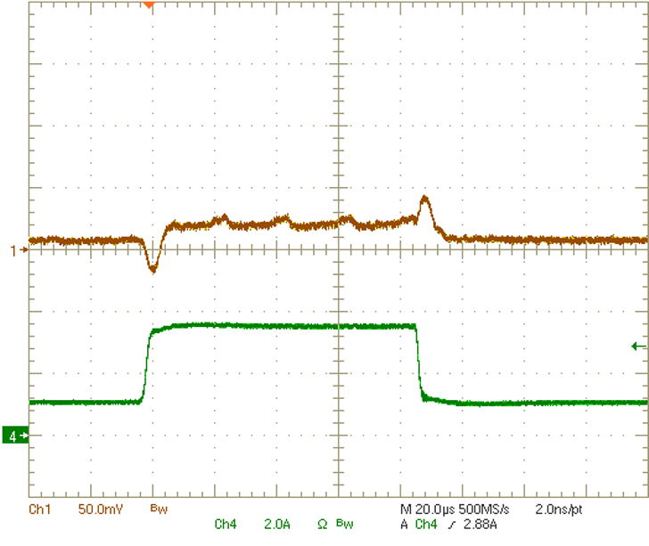
6.1.1.3 Application Curves
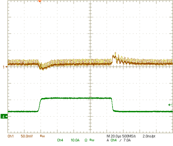
6.2 VIN 5-V Application
The PMIC can be operated by a 5-V input voltage to the system because the power path of the controller does not go through the device itself. The concept is simple: supply the controller VINs with the 5-V input, and supply the VSYS with a 5.8-V step-up of the 5 V with a boost or charge pump. The 5.8 V is recommended because the UVLO of the internal LDO5 is at 5.6 V and the device measures the voltage at VSYS and determines the optimum internal compensation and controller settings thus, it is ideal the VSYS be close to the VIN of the controllers.
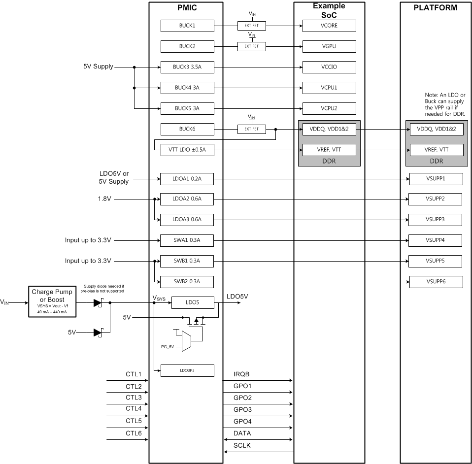 Figure 6-6 VIN 5-V Application
6.2.1 Design Requirements
The PMIC requires a step-up voltage from the 5-V input to 5.8 V for the VSYS supply. TI recommends keeping the VSYS near 5.8 V for optimization of the controllers.
Depending on the application use cases, the supply current to the VSYS can require from 40 mA with the drivers being supplied by the 5-V input to 440 mA with the drivers being supplied by the LDO5 and the LDOA1 being operated at max loading. This means that a charge pump may be used in some applications like the 5-V input but in others, a small boost may be required.
A Schottky diode from the 5-V input to the VSYS is recommended to ensure the VSYS is biased and the internal reference LDOs are on before the step-up regulator is enabled or fully ramped up. If the step-up cannot tolerate pre-bias condition then, 2 diodes may be needed to prevent the initial 5-V supply biasing the output of the step-up.
6.2.2 Design Procedure
To design a 5-V input application, first provide a step-up voltage from the 5-V input to the VSYS. Design the step-up to output a voltage near 5.8 V. Next, route the 5-V input to the controller and converter VINs. Thus, all power paths (all high currents) are routed through the controllers or directly to the converters. None of the high currents are required from the step-up supply. After the input stage is complete, the rest of the system can be designed as normal following the typical application procedure. Only the controller design is affected by the input voltage change.
6.2.2.1 Controller Design Procedure
Designing the controller can be broken down into the following steps:
- Design the output filter.
- Select the FETs.
- Select the bootstrap capacitor, same procedure as Section 6.1.1.2.1.4
- Select the input capacitors.
- Set the current limits. Will be very different values but, same procedure as Section 6.1.1.2.1.5
Controllers BUCK1, BUCK2, and BUCK6 require a 5-V supply and capacitors at their corresponding DRV5V_x_x pins. For most applications, the DRV5V_x_x input must come from the LDO5P0 pin to ensure uninterrupted supply voltage; a 2.2-µF, X5R, 20%, 10-V, or similar capacitor must be used for decoupling.
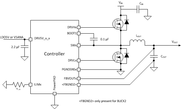 Figure 6-7 5-V Input Controller Diagram
6.2.2.1.1 Selecting the LC Output Filter
Selecting the inductor is the same as the typical application. Refer to Section 6.1.1.2.1.1 for desired inductor calculations.
Selection of the output capacitance is also the same as the typical design procedure, but due to the reduced VIN, the likely required minimum COUT will be larger. This is because the VL, or VIN – VOUT, is much smaller. Refer to Section 6.1.1.2.1.2 for output capacitance selection calculations.
6.2.2.1.2 Selecting the FETs
For lower current and lower input voltage applications, smaller lower-cost FETs can be selected with the trade off of RDSON and max VDS because the output power is reduced. The CSD85301Q2 is recommended for lower current applications. The CSD87381P is recommended for mid-range current applications.
6.2.2.1.3 Setting the Current Limit
The current-limiting resistor value must be chosen based on Equation 1.
6.2.2.1.4 Selecting the Input Capacitors
Due to the nature of the switching controller with a pulsating input current, a low ESR input capacitor is required for best input-voltage filtering and also for minimizing the interference with other circuits caused by high input-voltage spikes. For the controller, a typical 2.2-µF capacitor can be used for the DRV5V_x_x pin to handle the transients on the driver. For the FET input, 10 µF of input capacitance (after derating) is recommended for most applications. To achieve the low ESR requirement, a ceramic capacitor is recommended. However, the voltage rating and DC-bias characteristic of ceramic capacitors must be considered. For better input-voltage filtering, the input capacitor can be increased without any limit.
NOTE
Use the correct value for the ceramic capacitor capacitance after derating to achieve the recommended input capacitance.
TI recommends placing a ceramic capacitor as close as possible to the FET across the respective VIN and PGND pins of the FETs. The preferred capacitors for the controllers are two Murata GRM188R61A226ME15 (22-µF, 0603, 10-V, ±20%) or similar capacitors.
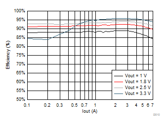
6.2.3 Application Curve
6.3 Do's and Don'ts
- Connect the LDO5V output to the DRV5V_x_x inputs for situations where an external 5-V supply is not initially available or is not available the entire time PMIC is on. If the external 5-V supply is always present, then DRV5V_x_x can be directly connected to remove the V5ANA-to-LDO5P0 load switch RDSON.
- Ensure that none of the control pins are potentially floating.
- Include 0-Ω resistors on the DRVH and BOOT pins of controllers on prototype boards, which allows for slowing the controllers if the system is unable to handle the noise generated by the large switching or if switching voltage is too large due to layout.
- Do not connect the V5ANA power input to a different source other than PVINx. A mismatch here causes reference circuits to regulate incorrectly.
- Do not supply the V5ANA power input before the VSYS. Reference biasing of the internal FETs may turn on the HS FET passing the input to the output until VSYS is biased.