ZHCSG44F June 2017 – October 2024 TPS650864
PRODUCTION DATA
- 1
- 1 特性
- 2 应用
- 3 说明
- 4 Device Comparison Table
- 5 Pin Configuration and Functions
-
6 Specifications
- 6.1 Absolute Maximum Ratings
- 6.2 ESD Ratings
- 6.3 Recommended Operating Conditions
- 6.4 Thermal Information
- 6.5 Electrical Characteristics: Total Current Consumption
- 6.6 Electrical Characteristics: Reference and Monitoring System
- 6.7 Electrical Characteristics: Buck Controllers
- 6.8 Electrical Characteristics: Synchronous Buck Converters
- 6.9 Electrical Characteristics: LDOs
- 6.10 Electrical Characteristics: Load Switches
- 6.11 Digital Signals: I2C Interface
- 6.12 Digital Input Signals (CTLx)
- 6.13 Digital Output Signals (IRQB, GPOx)
- 6.14 Timing Requirements
- 6.15 Switching Characteristics
- 6.16 Typical Characteristics
-
7 Detailed Description
- 7.1 Overview
- 7.2 Functional Block Diagram
- 7.3 TPS6508640 Design and Settings
- 7.4 TPS65086401 Design and Settings
- 7.5 TPS6508641 Design and Settings
- 7.6 TPS65086470 Design and Settings
- 7.7 SMPS Voltage Regulators
- 7.8 LDOs and Load Switches
- 7.9 Power Goods (PGOOD or PG) and GPOs
- 7.10 Power Sequencing and VR Control
- 7.11 Device Functional Modes
- 7.12 I2C Interface
- 7.13
Register Maps
- 7.13.1 Register Map Summary
- 7.13.2 DEVICEID1: 1st PMIC Device and Revision ID Register (offset = 00h) [reset = X]
- 7.13.3 DEVICEID2: 2nd PMIC Device and Revision ID Register (offset = 01h) [reset = X]
- 7.13.4 IRQ: PMIC Interrupt Register (offset = 02h) [reset = 0000 0000]
- 7.13.5 IRQ_MASK: PMIC Interrupt Mask Register (offset = 03h) [reset = 1111 1111]
- 7.13.6 PMICSTAT: PMIC Status Register (offset = 04h) [reset = 0000 0000]
- 7.13.7 SHUTDNSRC: PMIC Shut-Down Event Register (offset = 05h) [reset = 0000 0000]
- 7.13.8 BUCK1CTRL: BUCK1 Control Register (offset = 20h) [reset = X]
- 7.13.9 BUCK2CTRL: BUCK2 Control Register (offset = 21h) [reset = X]
- 7.13.10 BUCK3DECAY: BUCK3 Decay Control Register (offset = 22h) [reset = X]
- 7.13.11 BUCK3VID: BUCK3 VID Register (offset = 23h) [reset = X]
- 7.13.12 BUCK3SLPCTRL: BUCK3 Sleep Control VID Register (offset = 24h) [reset = X]
- 7.13.13 BUCK4CTRL: BUCK4 Control Register (offset = 25h) [reset = X]
- 7.13.14 BUCK5CTRL: BUCK5 Control Register (offset = 26h) [reset = X]
- 7.13.15 BUCK6CTRL: BUCK6 Control Register (offset = 27h) [reset = X]
- 7.13.16 LDOA2CTRL: LDOA2 Control Register (offset = 28h) [reset = X]
- 7.13.17 LDOA3CTRL: LDOA3 Control Register (offset = 29h) [reset = X]
- 7.13.18 DISCHCTRL1: 1st Discharge Control Register (offset = 40h) [reset = X]
- 7.13.19 DISCHCTRL2: 2nd Discharge Control Register (offset = 41h) [reset = X]
- 7.13.20 DISCHCTRL3: 3rd Discharge Control Register (offset = 42h) [reset = X]
- 7.13.21 PG_DELAY1: 1st Power Good Delay Register (offset = 43h) [reset = X]
- 7.13.22 FORCESHUTDN: Force Emergency Shutdown Control Register (offset = 91h) [reset = 0000 0000]
- 7.13.23 BUCK1SLPCTRL: BUCK1 Sleep Control Register (offset = 92h) [reset = X]
- 7.13.24 BUCK2SLPCTRL: BUCK2 Sleep Control Register (offset = 93h) [reset = X]
- 7.13.25 BUCK4VID: BUCK4 VID Register (offset = 94h) [reset = X]
- 7.13.26 BUCK4SLPVID: BUCK4 Sleep VID Register (offset = 95h) [reset = X]
- 7.13.27 BUCK5VID: BUCK5 VID Register (offset = 96h) [reset = X]
- 7.13.28 BUCK5SLPVID: BUCK5 Sleep VID Register (offset = 97h) [reset = X]
- 7.13.29 BUCK6VID: BUCK6 VID Register (offset = 98h) [reset = X]
- 7.13.30 BUCK6SLPVID: BUCK6 Sleep VID Register (offset = 99h) [reset = X]
- 7.13.31 LDOA2VID: LDOA2 VID Register (offset = 9Ah) [reset = X]
- 7.13.32 LDOA3VID: LDOA3 VID Register (offset = 9Bh) [reset = X]
- 7.13.33 BUCK123CTRL: BUCK1-3 Control Register (offset = 9Ch) [reset = X]
- 7.13.34 PG_DELAY2: 2nd Power Good Delay Register (offset = 9Dh) [reset = X]
- 7.13.35 SWVTT_DIS: SWVTT Disable Register (offset = 9Fh) [reset = X]
- 7.13.36 I2C_RAIL_EN1: 1st VR Pin Enable Override Register (offset = A0h) [reset = X]
- 7.13.37 I2C_RAIL_EN2/GPOCTRL: 2nd VR Pin Enable Override and GPO Control Register (offset = A1h) [reset = X]
- 7.13.38 PWR_FAULT_MASK1: 1st VR Power Fault Mask Register (offset = A2h) [reset = X]
- 7.13.39 PWR_FAULT_MASK2: 2nd VR Power Fault Mask Register (offset = A3h) [reset = X]
- 7.13.40 GPO1PG_CTRL1: 1st GPO1 PG Control Register (offset = A4h) [reset = X]
- 7.13.41 GPO1PG_CTRL2: 2nd GPO1 PG Control Register (offset = A5h) [reset = X]
- 7.13.42 GPO4PG_CTRL1: 1st GPO4 PG Control Register (offset = A6h) [reset = X]
- 7.13.43 GPO4PG_CTRL2: 2nd GPO4 PG Control Register (offset = A7h) [reset = X]
- 7.13.44 GPO2PG_CTRL1: 1st GPO2 PG Control Register (offset = A8h) [reset = X]
- 7.13.45 GPO2PG_CTRL2: 2nd GPO2 PG Control Register (offset = A9h) [reset = X]
- 7.13.46 GPO3PG_CTRL1: 1st GPO3 PG Control Register (offset = AAh) [reset = X]
- 7.13.47 GPO3PG_CTRL2: 2nd GPO3 PG Control Register (offset = ABh) [reset = X]
- 7.13.48 MISCSYSPG Register (offset = ACh) [reset = X]
- 7.13.49 LDOA1_SWB2_CTRL: LDOA1 and SWB2 Control Register (offset = AEh) [reset = X]
- 7.13.50 PG_STATUS1: 1st Power Good Status Register (offset = B0h) [reset = 0000 0000]
- 7.13.51 PG_STATUS2: 2nd Power Good Status Register (offset = B1h) [reset = 0000 0000]
- 7.13.52 PWR_FAULT_STATUS1: 1st Power Fault Status Register (offset = B2h) [reset = 0000 0000]
- 7.13.53 PWR_FAULT_STATUS2: 2nd Power Fault Status Register (offset = B3h) [reset = 0000 0000]
- 7.13.54 TEMPCRIT: Temperature Fault Status Register (offset = B4h) [reset = 0000 0000]
- 7.13.55 TEMPHOT: Temperature Hot Status Register (offset = B5h) [reset = 0000 0000]
- 7.13.56 OC_STATUS: Overcurrent Fault Status Register (offset = B6h) [reset = 0000 0000]
-
8 Applications, Implementation, and Layout
- 8.1 Application Information
- 8.2 Typical Application
- 8.3 Power Supply Coupling and Bulk Capacitors
- 8.4 Do's and Don'ts
- 9 Device and Documentation Support
- 10Revision History
- 11Mechanical, Packaging, and Orderable Information
7.5 TPS6508641 Design and Settings
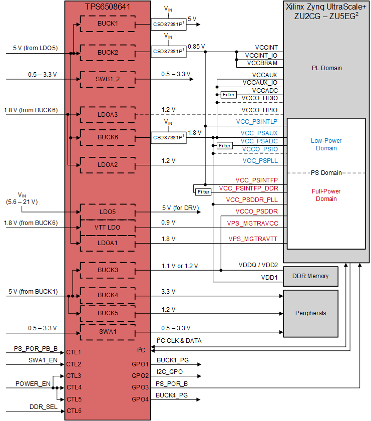
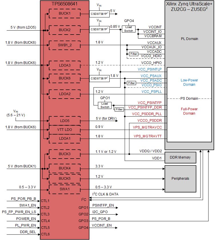
The TPS6508641 device is intended to power the lower range of the Xilinx Zynq Ultrascale+ platform. It removes the need for an external 5 V regulator when compared with the TPS65086401 device and also supports a wider variety of Zynq Ultrascale+ power states. Figure 7-9 shows a simple example block diagram for an always-on system, while Figure 7-10 shows a block diagram for full power domain flexibility. See Xilinx's Ultrascale Architecture PCB Design for explanation of the power supply configurations.


The power up and power down sequences can be seen in Figure 7-11 and Figure 7-12. Regulators and GPOs are enabled by combination of CTL pins and regulator power good signals.
 Figure 7-11 TPS6508641 Power-Up Sequence
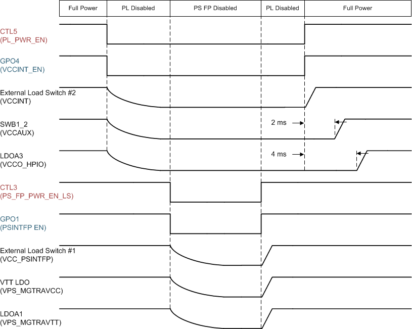
 Figure 7-13 TPS6508641 Low Power States
The TPS6508641 device is designed to be able to support always on and full power domain flexibility power modes. The low power states can be omitted if not required.
CTL4 is used to start the primary power sequence and CTL1, CTL3, and CTL5 should all be high initially to complete the power up sequence. For always-on case, CTL3 and CTL5 can be shorted with CTL4.
CTL6 is used to select BUCK3 voltage between BUCK3_VID and BUCK3_SLP_VID register bits. Logic level low will result in 1.2 V while logic level high will result in 1.1 V.
CTL2 is used to enable and disable SWA1 and is independent of the rest of the sequence.
When CTL1 is set low, GPO3 (PS_POR_B) is set low regardless of the power state and has 50 ms delay before going high after CTL1 goes high. It is used as a reset for the Zynq Ultrascale+ device. It can be pulled up to LDO3P3 (3.3 V) or BUCK6 (1.8 V) as preferred with a 10 kΩ resistor and a pushbutton can short this CTL pin to GND when MPSoC reset is desired.
GPO1 and GPO4 are used to control load switches when utilizing the low power modes. The load switches can be omitted for cases where low power modes are not necessary.
VTT LDO voltage used to power VPS_MGTRAVCC is configured to 0.9 V in order to support all variant speeds, including -3E designs. It is within the absolute voltage range and is not expected to impact performance for non-3E designs based on testing with the Ultra96 board. For more information on VPS_MGTRAVCC voltage, see Xilinx's Ultrascale Architecture PCB Design, Table 7-2 MPSoC PS Voltage Matrix by Speed/Temperature Grade.
A summary of the part number specific settings can be seen in Section 7.5.1.