ZHCSG44F June 2017 – October 2024 TPS650864
PRODUCTION DATA
- 1
- 1 特性
- 2 应用
- 3 说明
- 4 Device Comparison Table
- 5 Pin Configuration and Functions
-
6 Specifications
- 6.1 Absolute Maximum Ratings
- 6.2 ESD Ratings
- 6.3 Recommended Operating Conditions
- 6.4 Thermal Information
- 6.5 Electrical Characteristics: Total Current Consumption
- 6.6 Electrical Characteristics: Reference and Monitoring System
- 6.7 Electrical Characteristics: Buck Controllers
- 6.8 Electrical Characteristics: Synchronous Buck Converters
- 6.9 Electrical Characteristics: LDOs
- 6.10 Electrical Characteristics: Load Switches
- 6.11 Digital Signals: I2C Interface
- 6.12 Digital Input Signals (CTLx)
- 6.13 Digital Output Signals (IRQB, GPOx)
- 6.14 Timing Requirements
- 6.15 Switching Characteristics
- 6.16 Typical Characteristics
-
7 Detailed Description
- 7.1 Overview
- 7.2 Functional Block Diagram
- 7.3 TPS6508640 Design and Settings
- 7.4 TPS65086401 Design and Settings
- 7.5 TPS6508641 Design and Settings
- 7.6 TPS65086470 Design and Settings
- 7.7 SMPS Voltage Regulators
- 7.8 LDOs and Load Switches
- 7.9 Power Goods (PGOOD or PG) and GPOs
- 7.10 Power Sequencing and VR Control
- 7.11 Device Functional Modes
- 7.12 I2C Interface
- 7.13
Register Maps
- 7.13.1 Register Map Summary
- 7.13.2 DEVICEID1: 1st PMIC Device and Revision ID Register (offset = 00h) [reset = X]
- 7.13.3 DEVICEID2: 2nd PMIC Device and Revision ID Register (offset = 01h) [reset = X]
- 7.13.4 IRQ: PMIC Interrupt Register (offset = 02h) [reset = 0000 0000]
- 7.13.5 IRQ_MASK: PMIC Interrupt Mask Register (offset = 03h) [reset = 1111 1111]
- 7.13.6 PMICSTAT: PMIC Status Register (offset = 04h) [reset = 0000 0000]
- 7.13.7 SHUTDNSRC: PMIC Shut-Down Event Register (offset = 05h) [reset = 0000 0000]
- 7.13.8 BUCK1CTRL: BUCK1 Control Register (offset = 20h) [reset = X]
- 7.13.9 BUCK2CTRL: BUCK2 Control Register (offset = 21h) [reset = X]
- 7.13.10 BUCK3DECAY: BUCK3 Decay Control Register (offset = 22h) [reset = X]
- 7.13.11 BUCK3VID: BUCK3 VID Register (offset = 23h) [reset = X]
- 7.13.12 BUCK3SLPCTRL: BUCK3 Sleep Control VID Register (offset = 24h) [reset = X]
- 7.13.13 BUCK4CTRL: BUCK4 Control Register (offset = 25h) [reset = X]
- 7.13.14 BUCK5CTRL: BUCK5 Control Register (offset = 26h) [reset = X]
- 7.13.15 BUCK6CTRL: BUCK6 Control Register (offset = 27h) [reset = X]
- 7.13.16 LDOA2CTRL: LDOA2 Control Register (offset = 28h) [reset = X]
- 7.13.17 LDOA3CTRL: LDOA3 Control Register (offset = 29h) [reset = X]
- 7.13.18 DISCHCTRL1: 1st Discharge Control Register (offset = 40h) [reset = X]
- 7.13.19 DISCHCTRL2: 2nd Discharge Control Register (offset = 41h) [reset = X]
- 7.13.20 DISCHCTRL3: 3rd Discharge Control Register (offset = 42h) [reset = X]
- 7.13.21 PG_DELAY1: 1st Power Good Delay Register (offset = 43h) [reset = X]
- 7.13.22 FORCESHUTDN: Force Emergency Shutdown Control Register (offset = 91h) [reset = 0000 0000]
- 7.13.23 BUCK1SLPCTRL: BUCK1 Sleep Control Register (offset = 92h) [reset = X]
- 7.13.24 BUCK2SLPCTRL: BUCK2 Sleep Control Register (offset = 93h) [reset = X]
- 7.13.25 BUCK4VID: BUCK4 VID Register (offset = 94h) [reset = X]
- 7.13.26 BUCK4SLPVID: BUCK4 Sleep VID Register (offset = 95h) [reset = X]
- 7.13.27 BUCK5VID: BUCK5 VID Register (offset = 96h) [reset = X]
- 7.13.28 BUCK5SLPVID: BUCK5 Sleep VID Register (offset = 97h) [reset = X]
- 7.13.29 BUCK6VID: BUCK6 VID Register (offset = 98h) [reset = X]
- 7.13.30 BUCK6SLPVID: BUCK6 Sleep VID Register (offset = 99h) [reset = X]
- 7.13.31 LDOA2VID: LDOA2 VID Register (offset = 9Ah) [reset = X]
- 7.13.32 LDOA3VID: LDOA3 VID Register (offset = 9Bh) [reset = X]
- 7.13.33 BUCK123CTRL: BUCK1-3 Control Register (offset = 9Ch) [reset = X]
- 7.13.34 PG_DELAY2: 2nd Power Good Delay Register (offset = 9Dh) [reset = X]
- 7.13.35 SWVTT_DIS: SWVTT Disable Register (offset = 9Fh) [reset = X]
- 7.13.36 I2C_RAIL_EN1: 1st VR Pin Enable Override Register (offset = A0h) [reset = X]
- 7.13.37 I2C_RAIL_EN2/GPOCTRL: 2nd VR Pin Enable Override and GPO Control Register (offset = A1h) [reset = X]
- 7.13.38 PWR_FAULT_MASK1: 1st VR Power Fault Mask Register (offset = A2h) [reset = X]
- 7.13.39 PWR_FAULT_MASK2: 2nd VR Power Fault Mask Register (offset = A3h) [reset = X]
- 7.13.40 GPO1PG_CTRL1: 1st GPO1 PG Control Register (offset = A4h) [reset = X]
- 7.13.41 GPO1PG_CTRL2: 2nd GPO1 PG Control Register (offset = A5h) [reset = X]
- 7.13.42 GPO4PG_CTRL1: 1st GPO4 PG Control Register (offset = A6h) [reset = X]
- 7.13.43 GPO4PG_CTRL2: 2nd GPO4 PG Control Register (offset = A7h) [reset = X]
- 7.13.44 GPO2PG_CTRL1: 1st GPO2 PG Control Register (offset = A8h) [reset = X]
- 7.13.45 GPO2PG_CTRL2: 2nd GPO2 PG Control Register (offset = A9h) [reset = X]
- 7.13.46 GPO3PG_CTRL1: 1st GPO3 PG Control Register (offset = AAh) [reset = X]
- 7.13.47 GPO3PG_CTRL2: 2nd GPO3 PG Control Register (offset = ABh) [reset = X]
- 7.13.48 MISCSYSPG Register (offset = ACh) [reset = X]
- 7.13.49 LDOA1_SWB2_CTRL: LDOA1 and SWB2 Control Register (offset = AEh) [reset = X]
- 7.13.50 PG_STATUS1: 1st Power Good Status Register (offset = B0h) [reset = 0000 0000]
- 7.13.51 PG_STATUS2: 2nd Power Good Status Register (offset = B1h) [reset = 0000 0000]
- 7.13.52 PWR_FAULT_STATUS1: 1st Power Fault Status Register (offset = B2h) [reset = 0000 0000]
- 7.13.53 PWR_FAULT_STATUS2: 2nd Power Fault Status Register (offset = B3h) [reset = 0000 0000]
- 7.13.54 TEMPCRIT: Temperature Fault Status Register (offset = B4h) [reset = 0000 0000]
- 7.13.55 TEMPHOT: Temperature Hot Status Register (offset = B5h) [reset = 0000 0000]
- 7.13.56 OC_STATUS: Overcurrent Fault Status Register (offset = B6h) [reset = 0000 0000]
-
8 Applications, Implementation, and Layout
- 8.1 Application Information
- 8.2 Typical Application
- 8.3 Power Supply Coupling and Bulk Capacitors
- 8.4 Do's and Don'ts
- 9 Device and Documentation Support
- 10Revision History
- 11Mechanical, Packaging, and Orderable Information
7.6 TPS65086470 Design and Settings
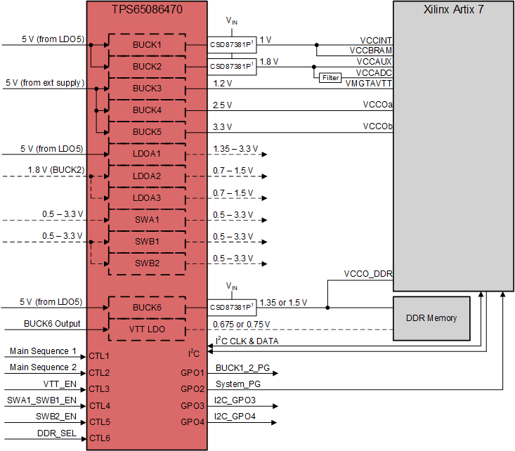
The TPS65086470 device is originally intended to power a Xilinx Artix 7 platform. Figure 7-14 shows an example block diagram for this system.

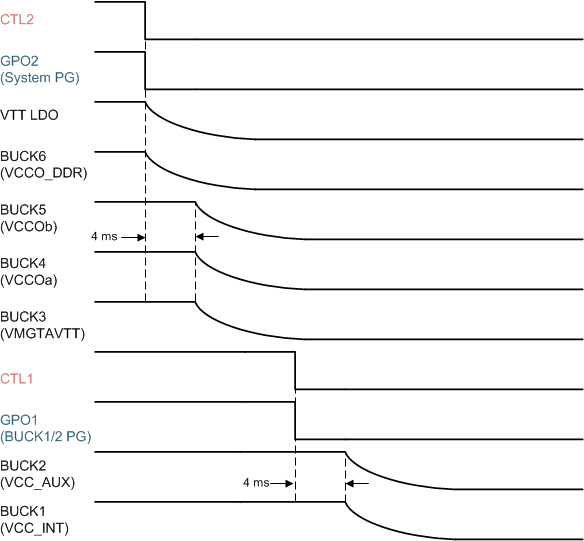
Figure 7-15 and Figure 7-16 show the power-up and power-down sequences. Regulators and GPOs are enabled by combination of CTL pins and regulator power good signals.
 Figure 7-15 TPS65086470 Power-Up Sequence
 Figure 7-16 TPS65086470 Power-Down Sequence
If CTL1 and CTL2 are set low at the same time, both sequences will occur simultaneously. If CTL1 is set low before CTL2, GPO1 and GPO2 will go low and remaining bucks will be disabled as their PG enable is lost. For example, as BUCK2 is disabled after 4 ms, BUCK3 will start it's 4 ms delay. As such it is recommended to not set CTL1 low before CTL2.
Additionally, CTL4 can be used to enable SWA1 and SWB1. CTL5 can be used to enable SWB2. LDOA2 and LDOA3 are controlled only by I2C.
A summary of the part number specific settings can be seen in Section 7.6.1.