ZHCSFJ2E September 2015 – October 2024 TPS65094
PRODUCTION DATA
- 1
- 1 特性
- 2 应用
- 3 说明
- 4 Device Options
- 5 Pin Configuration and Functions
-
6 Specifications
- 6.1 Absolute Maximum Ratings
- 6.2 ESD Ratings
- 6.3 Recommended Operating Conditions
- 6.4 Thermal Information
- 6.5 Electrical Characteristics: Total Current Consumption
- 6.6 Electrical Characteristics: Reference and Monitoring System
- 6.7 Electrical Characteristics: Buck Controllers
- 6.8 Electrical Characteristics: Synchronous Buck Converters
- 6.9 Electrical Characteristics: LDOs
- 6.10 Electrical Characteristics: Load Switches
- 6.11 Digital Signals: I2C Interface
- 6.12 Digital Input Signals (LDOLS_EN, SWA1_EN, THERMTRIPB, PMICEN, SLP_S3B, SLP_S4B, SLP_S0B)
- 6.13 Digital Output Signals (IRQB, RSMRSTB, PCH_PWROK, PROCHOT)
- 6.14 Timing Requirements
- 6.15 Switching Characteristics
- 6.16 Typical Characteristics
-
7 Detailed Description
- 7.1 Overview
- 7.2 Functional Block Diagram
- 7.3 Feature Description
- 7.4 Device Functional Modes
- 7.5 Programming
- 7.6
Register Maps
- 7.6.1 55
- 7.6.2 VENDORID: PMIC Vendor ID Register (offset = 00h) [reset = 0010 0010]
- 7.6.3 DEVICEID: PMIC Device and Revision ID Register (offset = 01h) [reset = OTP Dependent]
- 7.6.4 IRQ: PMIC Interrupt Register (offset = 02h) [reset = 0000 0000]
- 7.6.5 IRQ_MASK: PMIC Interrupt Mask Register (offset = 03h) [reset = 1111 1111]
- 7.6.6 PMICSTAT: PMIC Status Register (offset = 04h) [reset = 0000 0000]
- 7.6.7 OFFONSRC: PMIC Power Transition Event Register (offset = 05h) [reset = 0000 0000]
- 7.6.8 BUCK1CTRL: BUCK1 Control Register (offset = 20h) [reset = 0011 1000]
- 7.6.9 BUCK2CTRL: BUCK2 Control Register (offset = 21h) [reset = 0000 0000]
- 7.6.10 BUCK3CTRL: BUCK3 Control Register (offset = 23h) [reset = 0001 0001]
- 7.6.11 BUCK4CTRL: BUCK4 Control Register (offset = 25h) [reset = OTP Dependent]
- 7.6.12 BUCK5CTRL: BUCK5 Control Register (offset = 26h) [reset = OTP Dependent]
- 7.6.13 BUCK6CTRL: BUCK6 Control Register (offset = 27h) [reset = 0011 1101]
- 7.6.14 DISCHCNT1: Discharge Control1 Register (offset = 40h) [reset = 0101 0101]
- 7.6.15 DISCHCNT2: Discharge Control2 Register (offset = 41h) [reset = 0101 0101]
- 7.6.16 DISCHCNT3: Discharge Control3 Register (offset = 42h) [reset = 0000 0101]
- 7.6.17 POK_DELAY: PCH_PWROK Delay Register (offset = 43h) [reset = 0000 0111]
- 7.6.18 FORCESHUTDN: Force Emergency Shutdown Control Register (offset = 91h) [reset = 0000 0000]
- 7.6.19 BUCK4VID: BUCK4 VID Register (offset = 94h) [reset = 0010 1111]
- 7.6.20 BUCK5VID: BUCK5 VID Register (offset = 96h) [reset = 0100 1011]
- 7.6.21 BUCK6VID: BUCK6 VID Register (offset = 98h) [reset = OTP Dependent]
- 7.6.22 LDOA2VID: LDOA2 VID Register (offset = 9Ah) [reset = OTP Dependent]
- 7.6.23 LDOA3VID: LDOA3 VID Register (offset = 9Bh) [reset = OTP Dependent]
- 7.6.24 VR_CTRL1: BUCK1-3 Control Register (offset = 9Ch) [reset = OTP Dependent]
- 7.6.25 VR_CTRL2: VR Enable Register (offset = 9Eh) [reset = 0000 0000]
- 7.6.26 VR_CTRL3: VR Enable/Disable Register (offset = 9Fh) [reset = OTP Dependent]
- 7.6.27 GPO_CTRL: GPO Control Register (offset = A1h) [reset = 0010 0000]
- 7.6.28 PWR_FAULT_MASK1: VR Power Fault Mask1 Register (offset = A2h) [reset = 1100 0000]
- 7.6.29 PWR_FAULT_MASK2: VR Power Fault Mask2 Register (offset = A3h) [reset = 0011 0111]
- 7.6.30 DISCHCNT4: Discharge Control4 Register (offset = ADh) [reset = 0110 0001]
- 7.6.31 LDOA1CTRL: LDOA1 Control Register (offset = AEh) [reset = OTP Dependent]
- 7.6.32 PG_STATUS1: Power Good Status1 Register (offset = B0h) [reset = 0000 0000]
- 7.6.33 PG_STATUS2: Power Good Status2 Register (offset = B1h) [reset = 0000 0000]
- 7.6.34 TEMPHOT: Temperature Hot Status Register (offset = B5h) [reset = 0000 0000]
-
8 Application and Implementation
- 8.1 Typical Application
- 8.2 Specific Application for TPS650944
- 8.3 Dos and Don'ts
- Power Supply Recommendations
- 8.4 Layout
- 9 Device and Documentation Support
- 10Revision History
- 11Mechanical, Packaging, and Orderable Information
7.3.3.3 DVS
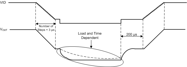
BUCK1–BUCK6 and LDOA1–3 support dynamic voltage scaling (DVS) for maximum system efficiency. The VR outputs can slew up and down in either 10-mV or 25-mV steps using the 7-bit voltage ID (VID) defined in Section 6.7, Electrical Characteristics: Buck Controllers, and Section 6.8, Electrical Characteristics: Synchronous Buck Converters. DVS slew rate is minimum 2.5 mV/µs. To meet the minimum slew rate, VID progresses to the next code at 3-µs (nom) interval per 10-mV step. When DVS is active, the VR is forced into PWM mode to ensure the output keeps track of VID code with minimal delay. Additionally, PGOOD is masked when DVS is in progress. Figure 7-5 shows an example of slew down and up from one VID to another.
 Figure 7-5 DVS Timing Diagram I
 As shown in Figure 7-6, if a BUCKx_VID[6:0] is set to 7b000 0000, the output voltage slews down to 0.5 V first, and then drifts down to 0 V as the SMPS stops switching. Subsequently, if a BUCKx_VID[6:0] is set to a value (neither 7b000 0000 nor 7b000 0001) when the output voltage is less than 0.5 V, the VR ramps up to 0.5 V first with soft-start kicking in, then it slews up to the target voltage in the aforementioned slew rate.
A fixed 200 µs of soft-start time is reserved for VOUT to reach 0.5 V. In this case, however, the SMPS is not forced into PWM mode because it otherwise could cause VOUT to droop momentarily if VOUT is drifting above 0.5 V for any reason.
 Figure 7-6 DVS Timing Diagram II