ZHCSFJ2E September 2015 – October 2024 TPS65094
PRODUCTION DATA
- 1
- 1 特性
- 2 应用
- 3 说明
- 4 Device Options
- 5 Pin Configuration and Functions
-
6 Specifications
- 6.1 Absolute Maximum Ratings
- 6.2 ESD Ratings
- 6.3 Recommended Operating Conditions
- 6.4 Thermal Information
- 6.5 Electrical Characteristics: Total Current Consumption
- 6.6 Electrical Characteristics: Reference and Monitoring System
- 6.7 Electrical Characteristics: Buck Controllers
- 6.8 Electrical Characteristics: Synchronous Buck Converters
- 6.9 Electrical Characteristics: LDOs
- 6.10 Electrical Characteristics: Load Switches
- 6.11 Digital Signals: I2C Interface
- 6.12 Digital Input Signals (LDOLS_EN, SWA1_EN, THERMTRIPB, PMICEN, SLP_S3B, SLP_S4B, SLP_S0B)
- 6.13 Digital Output Signals (IRQB, RSMRSTB, PCH_PWROK, PROCHOT)
- 6.14 Timing Requirements
- 6.15 Switching Characteristics
- 6.16 Typical Characteristics
-
7 Detailed Description
- 7.1 Overview
- 7.2 Functional Block Diagram
- 7.3 Feature Description
- 7.4 Device Functional Modes
- 7.5 Programming
- 7.6
Register Maps
- 7.6.1 55
- 7.6.2 VENDORID: PMIC Vendor ID Register (offset = 00h) [reset = 0010 0010]
- 7.6.3 DEVICEID: PMIC Device and Revision ID Register (offset = 01h) [reset = OTP Dependent]
- 7.6.4 IRQ: PMIC Interrupt Register (offset = 02h) [reset = 0000 0000]
- 7.6.5 IRQ_MASK: PMIC Interrupt Mask Register (offset = 03h) [reset = 1111 1111]
- 7.6.6 PMICSTAT: PMIC Status Register (offset = 04h) [reset = 0000 0000]
- 7.6.7 OFFONSRC: PMIC Power Transition Event Register (offset = 05h) [reset = 0000 0000]
- 7.6.8 BUCK1CTRL: BUCK1 Control Register (offset = 20h) [reset = 0011 1000]
- 7.6.9 BUCK2CTRL: BUCK2 Control Register (offset = 21h) [reset = 0000 0000]
- 7.6.10 BUCK3CTRL: BUCK3 Control Register (offset = 23h) [reset = 0001 0001]
- 7.6.11 BUCK4CTRL: BUCK4 Control Register (offset = 25h) [reset = OTP Dependent]
- 7.6.12 BUCK5CTRL: BUCK5 Control Register (offset = 26h) [reset = OTP Dependent]
- 7.6.13 BUCK6CTRL: BUCK6 Control Register (offset = 27h) [reset = 0011 1101]
- 7.6.14 DISCHCNT1: Discharge Control1 Register (offset = 40h) [reset = 0101 0101]
- 7.6.15 DISCHCNT2: Discharge Control2 Register (offset = 41h) [reset = 0101 0101]
- 7.6.16 DISCHCNT3: Discharge Control3 Register (offset = 42h) [reset = 0000 0101]
- 7.6.17 POK_DELAY: PCH_PWROK Delay Register (offset = 43h) [reset = 0000 0111]
- 7.6.18 FORCESHUTDN: Force Emergency Shutdown Control Register (offset = 91h) [reset = 0000 0000]
- 7.6.19 BUCK4VID: BUCK4 VID Register (offset = 94h) [reset = 0010 1111]
- 7.6.20 BUCK5VID: BUCK5 VID Register (offset = 96h) [reset = 0100 1011]
- 7.6.21 BUCK6VID: BUCK6 VID Register (offset = 98h) [reset = OTP Dependent]
- 7.6.22 LDOA2VID: LDOA2 VID Register (offset = 9Ah) [reset = OTP Dependent]
- 7.6.23 LDOA3VID: LDOA3 VID Register (offset = 9Bh) [reset = OTP Dependent]
- 7.6.24 VR_CTRL1: BUCK1-3 Control Register (offset = 9Ch) [reset = OTP Dependent]
- 7.6.25 VR_CTRL2: VR Enable Register (offset = 9Eh) [reset = 0000 0000]
- 7.6.26 VR_CTRL3: VR Enable/Disable Register (offset = 9Fh) [reset = OTP Dependent]
- 7.6.27 GPO_CTRL: GPO Control Register (offset = A1h) [reset = 0010 0000]
- 7.6.28 PWR_FAULT_MASK1: VR Power Fault Mask1 Register (offset = A2h) [reset = 1100 0000]
- 7.6.29 PWR_FAULT_MASK2: VR Power Fault Mask2 Register (offset = A3h) [reset = 0011 0111]
- 7.6.30 DISCHCNT4: Discharge Control4 Register (offset = ADh) [reset = 0110 0001]
- 7.6.31 LDOA1CTRL: LDOA1 Control Register (offset = AEh) [reset = OTP Dependent]
- 7.6.32 PG_STATUS1: Power Good Status1 Register (offset = B0h) [reset = 0000 0000]
- 7.6.33 PG_STATUS2: Power Good Status2 Register (offset = B1h) [reset = 0000 0000]
- 7.6.34 TEMPHOT: Temperature Hot Status Register (offset = B5h) [reset = 0000 0000]
-
8 Application and Implementation
- 8.1 Typical Application
- 8.2 Specific Application for TPS650944
- 8.3 Dos and Don'ts
- Power Supply Recommendations
- 8.4 Layout
- 9 Device and Documentation Support
- 10Revision History
- 11Mechanical, Packaging, and Orderable Information
7.5.1.1 F/S-Mode Protocol
The master initiates data transfer by generating a START condition. The START condition exists when a high-to-low transition occurs on the SDA line while SCL is high (see Figure 7-13). All I2C-compatible devices should recognize a START condition.
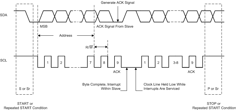
The master then generates the SCL
pulses and transmits the 7-bit address and the read/write direction bit R/W on the
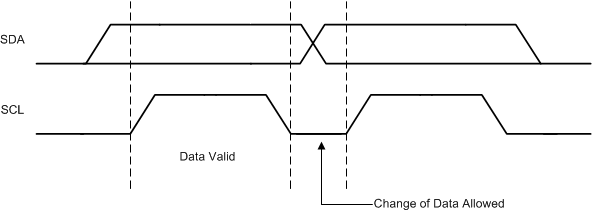
SDA line. During all transmissions, the master ensures that data is valid. A valid
data condition requires the SDA line to be stable during the entire high period of
the clock pulse (see
Figure 7-14). All devices recognize the address sent by the master and compare it to their
internal fixed addresses. Only the slave device with a matching address generates an
acknowledge (see Figure 7-15), by pulling the SDA line low during the entire high period of the ninth SCL
cycle. Upon detecting this acknowledge, the master identifies that the communication
link with a slave has been established.
The master generates further SCL cycles to either transmit data to the slave (R/W bit = 0) or receive data from the slave (R/W bit = 1). In either case, the receiver must acknowledge the data sent by the transmitter. An acknowledge signal can either be generated by the master or by the slave, depending on which one is the receiver. Any 9-bit valid data sequences consisting of 8-bit data and 1-bit acknowledge can continue as long as necessary.
To signal the end of the data transfer, the master generates a STOP condition by pulling the SDA line from low to high while the SCL line is high (see Figure 7-13). This STOP condition releases the bus and stops the communication link with the addressed slave. All I2C-compatible devices must recognize the STOP condition. Upon the receipt of a STOP condition, all devices detect that the bus is released, and they wait for a START condition followed by a matching address.
 Figure 7-13 START and STOP
Conditions
 Figure 7-14 Bit Transfer on the
I2C Bus
 Figure 7-15 Acknowledge on the
I2C Bus
 Figure 7-16 I2C Bus
Protocol
 Figure 7-17 I2C Interface WRITE
to TPS65094x in F/S Mode
 Figure 7-18 I2C Interface READ
from TPS65094x in F/S Mode (Only Repeated
START is Supported)