ZHCSFJ2E September 2015 – October 2024 TPS65094
PRODUCTION DATA
- 1
- 1 特性
- 2 应用
- 3 说明
- 4 Device Options
- 5 Pin Configuration and Functions
-
6 Specifications
- 6.1 Absolute Maximum Ratings
- 6.2 ESD Ratings
- 6.3 Recommended Operating Conditions
- 6.4 Thermal Information
- 6.5 Electrical Characteristics: Total Current Consumption
- 6.6 Electrical Characteristics: Reference and Monitoring System
- 6.7 Electrical Characteristics: Buck Controllers
- 6.8 Electrical Characteristics: Synchronous Buck Converters
- 6.9 Electrical Characteristics: LDOs
- 6.10 Electrical Characteristics: Load Switches
- 6.11 Digital Signals: I2C Interface
- 6.12 Digital Input Signals (LDOLS_EN, SWA1_EN, THERMTRIPB, PMICEN, SLP_S3B, SLP_S4B, SLP_S0B)
- 6.13 Digital Output Signals (IRQB, RSMRSTB, PCH_PWROK, PROCHOT)
- 6.14 Timing Requirements
- 6.15 Switching Characteristics
- 6.16 Typical Characteristics
-
7 Detailed Description
- 7.1 Overview
- 7.2 Functional Block Diagram
- 7.3 Feature Description
- 7.4 Device Functional Modes
- 7.5 Programming
- 7.6
Register Maps
- 7.6.1 55
- 7.6.2 VENDORID: PMIC Vendor ID Register (offset = 00h) [reset = 0010 0010]
- 7.6.3 DEVICEID: PMIC Device and Revision ID Register (offset = 01h) [reset = OTP Dependent]
- 7.6.4 IRQ: PMIC Interrupt Register (offset = 02h) [reset = 0000 0000]
- 7.6.5 IRQ_MASK: PMIC Interrupt Mask Register (offset = 03h) [reset = 1111 1111]
- 7.6.6 PMICSTAT: PMIC Status Register (offset = 04h) [reset = 0000 0000]
- 7.6.7 OFFONSRC: PMIC Power Transition Event Register (offset = 05h) [reset = 0000 0000]
- 7.6.8 BUCK1CTRL: BUCK1 Control Register (offset = 20h) [reset = 0011 1000]
- 7.6.9 BUCK2CTRL: BUCK2 Control Register (offset = 21h) [reset = 0000 0000]
- 7.6.10 BUCK3CTRL: BUCK3 Control Register (offset = 23h) [reset = 0001 0001]
- 7.6.11 BUCK4CTRL: BUCK4 Control Register (offset = 25h) [reset = OTP Dependent]
- 7.6.12 BUCK5CTRL: BUCK5 Control Register (offset = 26h) [reset = OTP Dependent]
- 7.6.13 BUCK6CTRL: BUCK6 Control Register (offset = 27h) [reset = 0011 1101]
- 7.6.14 DISCHCNT1: Discharge Control1 Register (offset = 40h) [reset = 0101 0101]
- 7.6.15 DISCHCNT2: Discharge Control2 Register (offset = 41h) [reset = 0101 0101]
- 7.6.16 DISCHCNT3: Discharge Control3 Register (offset = 42h) [reset = 0000 0101]
- 7.6.17 POK_DELAY: PCH_PWROK Delay Register (offset = 43h) [reset = 0000 0111]
- 7.6.18 FORCESHUTDN: Force Emergency Shutdown Control Register (offset = 91h) [reset = 0000 0000]
- 7.6.19 BUCK4VID: BUCK4 VID Register (offset = 94h) [reset = 0010 1111]
- 7.6.20 BUCK5VID: BUCK5 VID Register (offset = 96h) [reset = 0100 1011]
- 7.6.21 BUCK6VID: BUCK6 VID Register (offset = 98h) [reset = OTP Dependent]
- 7.6.22 LDOA2VID: LDOA2 VID Register (offset = 9Ah) [reset = OTP Dependent]
- 7.6.23 LDOA3VID: LDOA3 VID Register (offset = 9Bh) [reset = OTP Dependent]
- 7.6.24 VR_CTRL1: BUCK1-3 Control Register (offset = 9Ch) [reset = OTP Dependent]
- 7.6.25 VR_CTRL2: VR Enable Register (offset = 9Eh) [reset = 0000 0000]
- 7.6.26 VR_CTRL3: VR Enable/Disable Register (offset = 9Fh) [reset = OTP Dependent]
- 7.6.27 GPO_CTRL: GPO Control Register (offset = A1h) [reset = 0010 0000]
- 7.6.28 PWR_FAULT_MASK1: VR Power Fault Mask1 Register (offset = A2h) [reset = 1100 0000]
- 7.6.29 PWR_FAULT_MASK2: VR Power Fault Mask2 Register (offset = A3h) [reset = 0011 0111]
- 7.6.30 DISCHCNT4: Discharge Control4 Register (offset = ADh) [reset = 0110 0001]
- 7.6.31 LDOA1CTRL: LDOA1 Control Register (offset = AEh) [reset = OTP Dependent]
- 7.6.32 PG_STATUS1: Power Good Status1 Register (offset = B0h) [reset = 0000 0000]
- 7.6.33 PG_STATUS2: Power Good Status2 Register (offset = B1h) [reset = 0000 0000]
- 7.6.34 TEMPHOT: Temperature Hot Status Register (offset = B5h) [reset = 0000 0000]
-
8 Application and Implementation
- 8.1 Typical Application
- 8.2 Specific Application for TPS650944
- 8.3 Dos and Don'ts
- Power Supply Recommendations
- 8.4 Layout
- 9 Device and Documentation Support
- 10Revision History
- 11Mechanical, Packaging, and Orderable Information
7.3.5.3 Connected Standby Entry and Exit
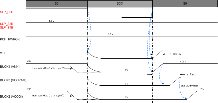
 Figure 7-9 Connected Standby Entry and Exit Sequence
S0 to S0iX (Connected Standby) entry and exit occurs when SLP_S0B is pulled low and high, respectively. In Connected Standby state, VTT LDO is turned off, but all PGOODs remain asserted. BUCK1–BUCK3 are not disabled, but instead stop switching while BUCK4–BUCK6 remain in regulation. SWB1_2 also stays enabled. On entry, BUCK2 and BUCK3 decay to 0 V with their VID registers retaining the last programmed values to which the BUCKs ramp back up on exit. The host can write to BUCK2CTRL and BUCK3CTRL registers regardless of the state of the SLP_S0B pin while SLP_S3B and SLP_S4B are high, which means that BUCK2 and BUCK3 can be changed to ramp to a different voltage upon exiting S0iX than they had when entering S0iX state. BUCK1 ramps back up to the default value (1.05 V).
Table 7-11 summarizes status of each VR in Connected Standby state.
| VR | S0 → S0IX | S0IX → S0 |
|---|---|---|
| BUCK1 (VNN) | 0 V | 1.05 V |
| BUCK2 (VCCGI) | 0 V | 0 V |
| BUCK3 (VCCRAM) | 0 V | 1.05 V |
| BUCK4 (V1P8A) | VID value | VID value |
| BUCK5 (V1P24A) | VID value | VID value |
| BUCK6 (VDDQ) | OTP dependent | OTP dependent |
| VTT LDO (VTT) | OFF | VDDQ / 2 |
| SWB1_2 | ON | ON |