SLVS849C July 2008 – September 2017 TPS65100-Q1
PRODUCTION DATA.
- 1 Features
- 2 Applications
- 3 Description
- 4 Revision History
- 5 Pin Configuration and Functions
- 6 Specifications
- 7 Detailed Description
-
8 Application and Implementation
- 8.1 Application Information
- 8.2
Typical Applications
- 8.2.1
Supply for a Typical Approximately 7-inch Display
- 8.2.1.1 Design Requirements
- 8.2.1.2
Detailed Design Procedure
- 8.2.1.2.1
Boost Converter Design Procedure
- 8.2.1.2.1.1 Inductor Selection
- 8.2.1.2.1.2 Output Capacitor Selection
- 8.2.1.2.1.3 Input Capacitor Selection
- 8.2.1.2.1.4 Rectifier Diode Selection
- 8.2.1.2.1.5 Converter Loop Design and Stability
- 8.2.1.2.1.6 Design Procedure Quick Steps
- 8.2.1.2.1.7 Setting the Output Voltage and Selecting the Feedforward Capacitor
- 8.2.1.2.2 Negative Charge Pump
- 8.2.1.2.3 Positive Charge Pump
- 8.2.1.2.4 VCOM Buffer
- 8.2.1.2.5 Linear Regulator Controller
- 8.2.1.2.1
Boost Converter Design Procedure
- 8.2.1.3 Application Curves
- 8.2.2 Supply for a Typical Approximately 8-inch Display
- 8.2.1
Supply for a Typical Approximately 7-inch Display
- 9 Power Supply Recommendations
- 10Layout
- 11Device and Documentation Support
- 12Mechanical, Packaging, and Orderable Information
10 Layout
10.1 Layout Guidelines
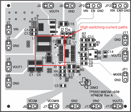
For all switching power supplies, the layout is an important step in the design, especially at high-peak currents and switching frequencies. If the layout is not carefully designed, the regulator might show stability and EMI problems. TI recommends the following PCB layout guidelines for the TPS65100-Q1 device:
- Connect PGND and AGND together on the same ground plane.
- Connect all capacitor grounds and PGND together on a common ground plane.
- Place the input filter capacitor as close as possible to the input pin of the IC.
- Route first the traces carrying high-switching currents with wide and short traces.
- Isolate analog signal paths from power paths.
- If vias are necessary, try to use more than one in parallel to decrease parasitics, especially for power traces.
- Solder the thermal pad to the PCB for good thermal performance
10.2 Layout Example
 Figure 20. Layout Example
10.3 Thermal Considerations
An influential component of thermal performance of a package is board design. To take full advantage of the heat dissipation abilities of the PowerPAD package with exposed thermal die, a board that acts similar to a heat sink and allows the use of an exposed (and solderable) deep downset pad should be used. For further information, see PowerPAD Thermally Enhanced Package, SLMA002, and PowerPAD Made Easy, SLMA004.