SLVS496D SEPTEMBER 2003 – August 2016 TPS65100 , TPS65101 , TPS65105
PRODUCTION DATA.
- 1 Features
- 2 Applications
- 3 Description
- 4 Revision History
- 5 Device Options
- 6 Pin Configuration and Functions
- 7 Specifications
- 8 Detailed Description
- 9 Application and Implementation
- 10Power Supply Recommendations
- 11Layout
- 12Device and Documentation Support
- 13Mechanical, Packaging, and Orderable Information
封装选项
请参考 PDF 数据表获取器件具体的封装图。
机械数据 (封装 | 引脚)
- RGE|24
- PWP|24
散热焊盘机械数据 (封装 | 引脚)
订购信息
9 Application and Implementation
NOTE
Information in the following applications sections is not part of the TI component specification, and TI does not warrant its accuracy or completeness. TI’s customers are responsible for determining suitability of components for their purposes. Customers should validate and test their design implementation to confirm system functionality.
9.1 Application Information
The TPS6510x series provides all three voltages that are required for (TFT) LCD displays. The auxiliary linear regulator controller can be used to generate a 3.3-V logic power rail for systems powered by a 5-V supply rail only. Additionally it has an integrated VCOM buffer to power the LCD backplane.
9.2 Typical Applications
Figure 15 shows a typical application circuit for a display panel power by a 5-V supply rail. It generates up to 350 mA at 15 V to drive the source driver and 20 mA at 30 V and –12 V to drive the gate drivers.
.gif) Figure 15. Typical Application Circuit
Figure 15. Typical Application Circuit
9.2.1 Design Requirements
Table 1 shows the design parameters for this example.
Table 1. Design Parameters
| PARAMETER | VALUE | |
|---|---|---|
| VI | Input supply voltage | 3.3 V |
| VO1 | Boost converter output voltage and current | 10 V at 300 mA |
| VO1(PP) | Boost converter peak-to-peak output voltage ripple | 1% = 10 mV |
| V(SW) | Switch voltage drop | 0.5 V |
| VF | Schottky diode forward voltage drop | 0.8 V |
| VO2 | Positive charge pump output voltage and current | 23 V at 20 mA |
| VO2(PP) | Positive charge pump peak-to-peak output voltage ripple | 100 mV |
| VO3 | Negative charge pump output voltage and current | –5 V at 20 mA |
| VO3(PP) | Negative charge pump peak-to-peak output voltage ripple | 100 mV |
9.2.2 Detailed Design Procedure
9.2.2.1 Boost Converter Design Procedure
The first step in the design procedure is to calculate the maximum possible output current of the main boost converter = 10 V.
- Duty cycle:
- Average inductor current:
- Inductor peak-to-peak ripple current:
- Peak switch current:


The integrated switch, the inductor and the external Schottky diode must be able to handle the peak switch current. The calculated peak switch current has to be equal or lower than the minimum N-MOSFET switch current limit (Q1) as specified in the electrical characteristics table (1.6 A for the TPS65100/01 and 0.96 A for the TPS65105).
If the peak switch current is higher, then the converter cannot support the required load current. This calculation must be done for the minimum input voltage where the peak switch current is highest. The calculation includes conduction losses like switch rDS(on) and diode forward drop voltage losses. Additional switching losses, inductor core and winding losses, etc., require a slightly higher peak switch current in the actual application. The above calculation still allows an estimate for a good design and component selection.
9.2.2.1.1 Inductor Selection
Several inductors work with the TPS6510x series. Especially with the external compensation, the performance can be adjusted to the specific application requirements. The main parameter for inductor selection is the saturation current of the inductor which should be higher than the peak switch current as calculated above with additional margin to cover for heavy load transients and extreme start-up conditions. Another method is to choose the inductor with a saturation current at least as high as the minimum switch current limit of 1.6 A for the TPS65100/01 and 0.96 A for the TPS65105. The different switch current limits allow selection of a physically smaller inductor when less output current is required. The second important parameter is inductor DC resistance.
Usually, the lower the DC resistance, the higher the efficiency. However, inductor DC resistance, is not the only parameter determining the efficiency. Especially for a boost converter where the inductor is the energy storage element the type and material of the inductor influences the efficiency as well. Especially at the high switching frequency of 1.6 MHz, inductor core losses, proximity effects, and skin effects become more important. Usually, an inductor with a larger form factor yields higher efficiency. The efficiency difference between different inductors can vary between 2% to 10%.
For the TPS6510x series, inductor values between 3.3 μH and 6.8 μH are a good choice but other values can be used as well. Possible inductors are shown in Table 2.
Table 2. Inductor Selection
| DEVICE | INDUCTOR VALUE | COMPONENT SUPPLIER | DIMENSIONS / mm | ISAT / DCR |
|---|---|---|---|---|
| TPS65100 | 4.7 μH | Coilcraft DO1813P-472HC | 8,89 x 6,1 x 5 | 2.6 A/54 mΩ |
| 4.2 μH | Sumida CDRH5D28 4R2 | 5,7 x 5,7 x 3 | 2.2 A/23 mΩ | |
| 4.7 μH | Sumida CDC5D23 4R7 | 6 x 6 x 2,5 | 1.6 A/48 mΩ | |
| 3.3 μH | Wuerth Elektronik 744042003 | 4,8 x 4,8 x 2 | 1.8 A/65 mΩ | |
| 4.2 μH | Sumida CDRH6D12 4R2 | 6,5 x 6,5 x 1,5 | 1.8 A/60 mΩ | |
| 3.3 μH | Sumida CDRH6D12 3R3 | 6,5 x 6,5 x 1,5 | 1.9 A/50 mΩ | |
| TPS65105 | 3.3 μH | Sumida CDPH4D19 3R3 | 5,1 x 5,1 x 2 | 1.5 A/26 mΩ |
| 3.3 μH | Coilcraft DO1606T-332 | 6,5 x 5,2 x 2 | 1.4 A/120 mΩ | |
| 3.3 μH | Sumida CDRH2D18/HP 3R3 | 3,2 x 3,2 x 2 | 1.45 A/69 mΩ | |
| 4.7 μH | Wuerth Elektronik 744010004 | 5,5 x 3,5 x 1 | 1.0 A/260 mΩ | |
| 3.3 μH | Coilcraft LPO6610-332M | 6,6 x 5,5 x 1 | 1.3 A/160 mΩ |
9.2.2.1.2 Output Capacitor Selection
For the best output voltage filtering, a low ESR output capacitor is recommended. Ceramic capacitors have a low ESR value, but depending on the application, tantalum capacitors can be used as well. A 22-μF ceramic output capacitor works for most of the applications. Higher capacitor values can be used to improve the load transient regulation. See Table 3 for selection of the output capacitor. The output voltage ripple can be calculated as:

where
- I(SW)M = Peak switch current as calculated in the previous section with I(SW)M
- L = Selected inductor value
- IO = Normal load current
- fosc = Switching frequency
- VF = Rectifier diode forward voltage (typical 0.3 V)
- CO = Selected output capacitor
- ESR = Output capacitor ESR value
9.2.2.1.3 Input Capacitor Selection
For good input voltage filtering, low ESR ceramic capacitors are recommended. A 22-μF ceramic input capacitor is sufficient for most of the applications. For better input voltage filtering, this value can be increased. See Table 3 for input capacitor recommendations.
Table 3. Input and Output Capacitors Selection
| CAPACITOR | VOLTAGE RATING | COMPONENT SUPPLIER | COMMENTS |
|---|---|---|---|
| 22 μF/1210 | 16 V | Taiyo Yuden EMK325BY226MM | output capacitor CO |
| 22 μF/1206 | 6.3 V | Taiyo Yuden JMK316BJ226 | input capacitor CI |
9.2.2.1.4 Rectifier Diode Selection
A Schottky diode is recommended to achieve good efficiency as the forward voltage drop is lower than of silicon diodes. The following table shows criteria which should be considered when choosing the rectifier diode:
Table 4. Rectifier Diode Selection Requirements
| PARAMETER | VALUE | Comment |
|---|---|---|
| Voltage Rating | ≥ VO1(M) | Higher than maximum output voltage of boost converter |
| Average Forward Current | ≥ IO | Higher than the output current |
| Peak Current | > IL(PP) | Higher than the inductor peak current |
| Forward voltage drop, reverse leakage current | Low as possible | For good efficiency |
Possible diodes are: On Semiconductor MBRM120L, Microsemi UPS120E, and Fairchild Semiconductor MBRS130L.
9.2.2.1.5 Converter Loop Design and Stability
The TPS6510x series converter loop can be externally compensated and allows access to the internal transconductance error amplifier output at the COMP pin. A small feedforward capacitor across the upper feedback resistor divider speeds up the circuit as well. To test the converter stability and load transient performance of the converter, a load step from 50 mA to 250 mA is applied, and the output voltage of the converter is monitored. Applying load steps to the converter output is a good tool to judge the stability of such a boost converter. Please refer to SLVA381 to understand the relationship between the phase margin in an AC loop response and the ringing in a load-step
9.2.2.1.6 Design Procedure Quick Steps
- Select the feedback resistor divider to set the output voltage.
- Select the feedforward capacitor to place a zero at 50 kHz.
- Select the compensation capacitor on pin COMP. The smaller the value, the higher the low frequency gain.
- Use a 50-kΩ potentiometer in series to Cc and monitor VO1 during load transients. Fine tune the load transient by adjusting the potentiometer. Select a resistor value that comes closest to the potentiometer resistor value. This needs to be done at the highest VI and highest load current since the stability is most critical at these conditions.
9.2.2.1.7 Setting the Output Voltage and Selecting the Feedforward Capacitor
The output voltage is set by the external resistor divider and is calculated as:

Across the upper resistor a bypass capacitor is required to speed up the circuit during load transients as shown in Figure 16.
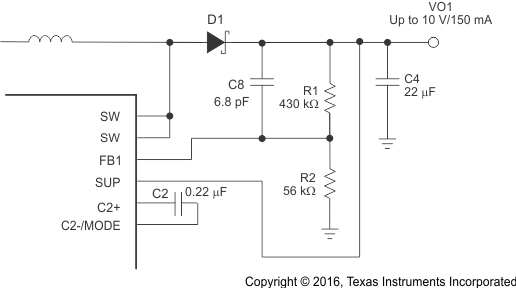 Figure 16. Feedforward Capacitor
Together with R1 the bypass capacitor C8 sets a zero in the control loop at approximately 50 kHz:

A value closest to the calculated value should be used. Larger feedforward capacitor values reduce the load regulation of the converter and cause DC voltage changes as shown in Figure 17.
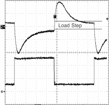 Figure 17. Load Regulation Caused by a Too Large Feedforward Capacitor Value
9.2.2.2 Negative Charge Pump
The negative charge pump provides a regulated output voltage by inverting the main output voltage VO1. The negative charge pump output voltage is set with external feedback resistors.
The maximum load current of the negative charge pump depends on the voltage drop across the external Schottky diodes, the internal on resistance of the charge pump MOSFETS Q8 and Q9, and the impedance of the flying capacitor C12. When the voltage drop across these components is larger than the voltage difference from VO1 to VO2, the charge pump is in dropout, providing the maximum possible output current.
Therefore, the higher the voltage difference between VO1 and VO2, the higher the possible load current. See Figure 12 for the possible output current versus boost converter voltage VO1.

Setting the output voltage:


The lower feedback resistor value R4 should be in a range between 40 kΩ to 120 kΩ or the overall feedback resistance should be within 500 kΩ to 1 MΩ. Smaller values load the reference too heavily and larger values may cause stability problems. The negative charge pump requires two external Schottky diodes. The peak current rating of the Schottky diode has to be twice the load current of the output. For a 20-mA output current, the dual Schottky diode BAT54 or similar is a good choice.
9.2.2.3 Positive Charge Pump
The positive charge pump can be operated in a voltage doubler mode or a voltage tripler mode depending on the configuration of the C2+ and C2-/MODE pins. To operate in a voltage doubler leave the C2+ pin open and connect C2-/MODE to GND. To operate the charge pump in the voltage tripler mode, a flying capacitor needs to be connected between C2+ and C2-/MODE.
The maximum load current of the positive charge pump depends on the voltage drop across the internal Schottky diodes, the internal on resistance of the charge pump MOSFETS, and the impedance of the flying capacitor. When the voltage drop across these components is larger than the voltage difference VO1 x 2 to VO3 (doubler mode) or VO1 x 3 to VO3 (tripler mode), then the charge pump is in dropout, providing the maximum possible output current. Therefore, the higher the voltage difference between 2 x VO1 or 3 x VO1 to VO3, the higher the possible load current. See Figure 13 and Figure 14 for the output current versus boost converter voltage VO1 and the following calculations. The following graph shows voltage ranges of a doubler and tripler depending of the boost converter voltage VO1.
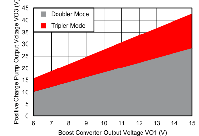 Figure 18. Positive Charge Pump – Output Ranges for IO = 20 mA
Table 5 gives first order formulas to calculate the minimum and maximum output voltages of the positive charge pump.
Table 5. Voltage Limitation Positive Charge Pump
| MODE | EQUATION | |
|---|---|---|
| Doubler | Minimum output voltage | VO3(min_d) = VO1 |
| Maximum output voltage | VO3(max_d) = 2 × VO1 – (2 × VF + 2 × IO·(2 × rDS(on)Q5 + rDS(on)Q3 + rDS(on)Q4 )) | |
| Tripler | Minimum output voltage | VO3(min_t) = VO3(max_d) |
| Maximum output voltage | VO3(max_t) = 3 × VO1 – (4 × VF + 2 × IO (3 × rDS(on)Q5 + rDS(on)Q3 + rDS(on)Q4 )) | |
The output voltage is set by the external resistor divider and is calculated as:


9.2.2.4 VCOM Buffer
The VCOM buffer is typically used to drive the backplane of a TFT panel. The VCOM output voltage is typically set to half of the main output voltage VO1 plus a small shift to implement the specific compensation voltage. The TFT video signal gets coupled through the TFT storage capacitor plus the LCD cell capacitance to the output of the VCOM buffer. Because of these, short current pulses in the positive and negative direction appear at the output of the VCOM buffer. To minimize the output voltage ripple caused by the current pulses, a transconductance amplifier having a current source output and an output capacitor is used. The output capacitor supports the high frequency part of the current pulses drawn from the LCD panel. The VCOM buffer only needs to handle the low frequency portion of the current pulses. A 1-μF ceramic output capacitor is sufficient for most of the applications.
The VCOM buffer has an integrated soft start to avoid voltage drops on VO1 during start-up. The soft start is implemented as such that the VCOMIN is held low until the VCOM buffer is fully biased and the common mode range is reached. Then the positive input is released and the VCOM buffer output slowly comes up. Usually a 1-nF capacitor on VCOMIN to GND is used to filter high frequency noise coupled in from VO1. The size of this capacitor together with the upper feedback resistor value determines the start-up time. The larger the capacitor from VCOMIN to GND, the slower the start-up time.
9.2.3 Application Curves
Table 6 lists the application curves.
Table 6. Table of Graphs
| FIGURE | |||
|---|---|---|---|
| MAIN BOOST CONVERTER (VOUT1) | |||
| PWM operation at light load | Figure 7 | ||
| Load transient response, CO = 22 μF | Figure 8 | ||
| Load transient response, CO = 2 x 22 μF | Figure 9 | ||
| Power-up sequencing | Figure 10 | ||
| Soft start VO1 | Figure 11 | ||
| NEGATIVE CHARGE PUMP | |||
| IOM | VO2 Maximum load current | vs Output voltage VO1 | Figure 12 |
| POSITIVE CHARGE PUMP | |||
| IOM | VO3 Maximum load current | vs Output voltage VO1 (doubler mode) | Figure 13 |
| IOM | VO3 Maximum load current | vs Output voltage VO1 (tripler mode) | Figure 14 |
9.3 System Examples
9.3.1 Notebook Supply
Figure 19 shows a typical application circuit suitable to supply (TFT) LCD displays in notebook applications. The circuit is designed to operate from a single-cell Li-Ion battery and generates output voltages for the source driver VO1 of 10 V, for the gate driver VO2 of –5 V and VO3 of 23 V and a VCOM voltage of VO1/2.
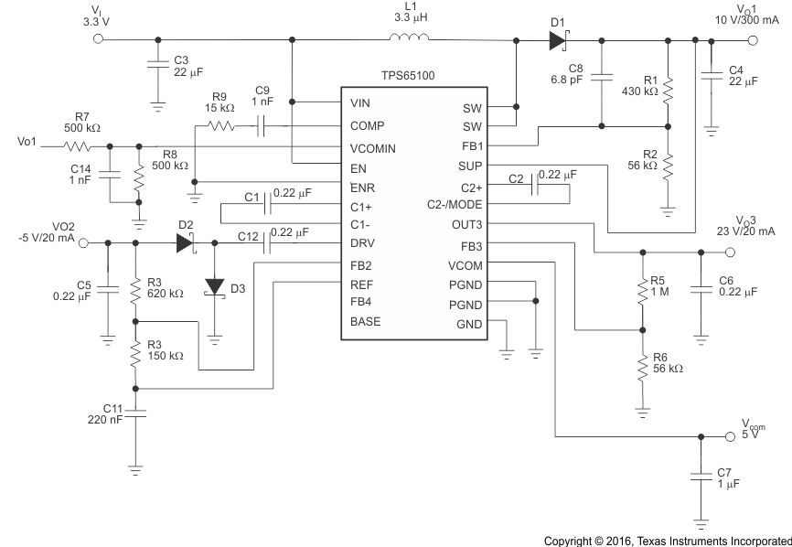 Figure 19. Typical Application, Notebook Supply Diagram
9.3.2 Monitor Supply
Figure 20 shows a typical application circuit suitable to supply (TFT) LCD displays in monitor applications. The circuit is designed to operate by a 5-V power rail and generates output voltages for the source driver VO1 of 13.5 V, for the gate driver VO2 of –7 V and VO3 of 23 V and a VCOM voltage of VO1/2. Additionally monitor applications also require a supply voltage for the digital part that is provided from VO4 of 3.3 V.
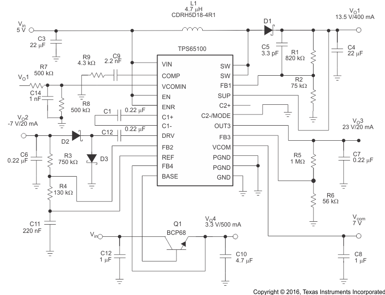 Figure 20. Typical Application, Monitor Supply Diagram