ZHCSQG4E March 2004 – April 2022 TPS65130 , TPS65131
PRODUCTION DATA
- 1 特性
- 2 应用
- 3 说明
- 4 Revision History
- 5 Pin Configuration and Functions
- 6 Specifications
- 7 Detailed Description
-
8 Applications and Implementation
- 8.1 Application Information
- 8.2
Typical Application
- 8.2.1 Design Requirements
- 8.2.2 Detailed Design Procedure
- 8.2.3 Analog Supply Filter
- 8.2.4 Application Curves
- 9 Layout
- 10Device and Documentation Support
- 11Mechanical, Packaging, and Orderable Information
封装选项
请参考 PDF 数据表获取器件具体的封装图。
机械数据 (封装 | 引脚)
- RGE|24
散热焊盘机械数据 (封装 | 引脚)
- RGE|24
订购信息
8.2.4 Application Curves
Table 8-5 Table of Figures
| FIGURE | DESCRIPTION |
|---|---|
| Figure 8-2 | TPS65130 efficiency versus output current, VPOS= 5 V |
| Figure 8-3 | TPS65131 efficiency versus output current, VPOS= 5 V |
| Figure 8-4 | TPS65130 efficiency versus output current, VPOS= 8 V |
| Figure 8-5 | TPS65131 efficiency versus output current, VPOS= 10 V |
| Figure 8-6 | TPS65130 efficiency versus output current, VPOS= 12 V |
| Figure 8-7 | TPS65131 efficiency versus output current, VPOS= 15 V |
| Figure 8-8 | TPS65130 efficiency versus output current, VNEG= –4 V, (VIN = 4 V, 3 V) |
| Figure 8-9 | TPS65131 efficiency versus output current, VNEG= –4 V, (VIN = 5 V, 3 V) |
| Figure 8-10 | TPS65130 efficiency versus output current, VNEG= –8 V, (VIN = 4.2 V, 3 V) |
| Figure 8-11 | TPS65131 efficiency versus output current, VNEG= –10 V, (VIN = 5 V, 3 V) |
| Figure 8-12 | TPS65130 efficiency versus output current, VNEG= –10 V, (VIN = 4.2 V, 3 V) |
| Figure 8-13 | TPS65131 efficiency versus output current, VNEG= –15 V, (VIN = 5 V, 3 V) |
| Figure 8-14 | TPS65130 efficiency versus input voltage, VPOS= 5 V in power-save mode |
| Figure 8-15 | TPS65130 efficiency versus input voltage, VPOS= 8 V in power-save mode |
| Figure 8-16 | TPS65130 efficiency versus input voltage, VPOS= 12 V in power-save mode |
| Figure 8-17 | TPS65130 efficiency versus input voltage, VNEG= –4 V in power-save mode |
| Figure 8-18 | TPS65130 efficiency versus input voltage, VNEG= –8 V in power-save mode |
| Figure 8-19 | TPS65130 efficiency versus input voltage, VNEG= –10 V in power-save mode |
| Figure 8-20 | TPS65130 efficiency versus output current, VO= 13.5 V (+9 V, –4.5 V), (VIN = 4.2 V, 3 V) |
| Figure 8-21 | TPS65131 efficiency versus output current, VO= 30 V (±15 V, (VIN 5 V, 3 V) |
| Figure 8-22 | TPS65130 efficiency versus input voltage, VO= 13.5 V (9 V, –4.5 V) in power save mode |
| Figure 8-23 | TPS65130 output voltage versus output current, VPOS= 5 V, VIN = 3 V |
| Figure 8-24 | TPS65131 output voltage versus output current, VPOS= 5 V, VIN = 4.2 V |
| Figure 8-25 | TPS65130 output voltage versus output current, VPOS= 8 V, VIN = 3 V |
| Figure 8-26 | TPS65131 output voltage versus output current, VPOS= 10 V, VIN = 5 V |
| Figure 8-27 | TPS65130 output voltage versus output current, VPOS= 12 V (VIN = 3 V) |
| Figure 8-28 | TPS65131 output voltage versus output current, VPOS= 15 V (VIN = 5 V) |
| Figure 8-29 | TPS65130 output voltage versus output current, VNEG= –4 V, VIN = 3 V |
| Figure 8-30 | TPS65131 output voltage versus output current, VNEG= –4 V, VIN = 5 V |
| Figure 8-31 | TPS65130 output voltage versus output current, VNEG= –8 V, VIN = 3 V |
| Figure 8-32 | TPS65131 output voltage versus output current, VNEG= –10 V, VIN = 5 V |
| Figure 8-33 | TPS65130 output voltage versus output current, VNEG= –10 V, VIN = 3 V |
| Figure 8-34 | TPS65131 output voltage versus output current, VNEG= –15 V, VIN = 5 V |
| Figure 8-35 | Positive output voltage in continuous current mode |
| Figure 8-36 | Negative output voltage in continuous current mode |
| Figure 8-37 | Positive output voltage at power-save mode disabled |
| Figure 8-38 | Negative output voltage at power-save mode disabled |
| Figure 8-39 | Positive output voltage in power-save mode, VI = 3.6 V, VPOS = 5.5 V |
| Figure 8-40 | Negative output voltage in power-save mode, VI = 3.6 V, VNEG = –8 V |
| Figure 8-41 | Load transient response, VI = 3.6 V, VPOS = 8 V |
| Figure 8-42 | Load transient response, VI = 3.6 V, VNEG = –8 V |
| Figure 8-43 | Line transient response, VI = 3.6 V to 4.2 V, VPOS = 8 V |
| Figure 8-44 | Line transient response, VI = 3.6 V to 4.2 V, VNEG = –8 V |
| Figure 8-45 | Start-up after enable, VPOS = 8 V, VI = 3.6 V |
| Figure 8-46 | Start-up after enable, VNEG = –8 V, VI = 3.6 V |
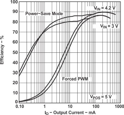 Figure 8-2 TPS65130 Efficiency vs Output Current
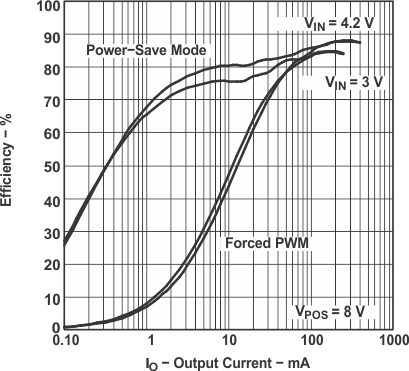 Figure 8-4 TPS65130 Efficiency vs Output Current
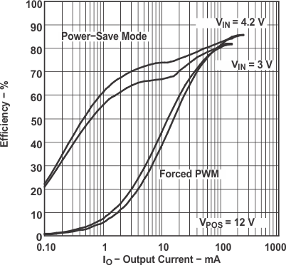 Figure 8-6 TPS65130 Efficiency vs Output Current
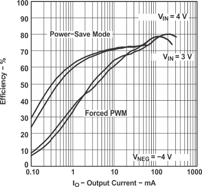 Figure 8-8 TPS65130 Efficiency vs Output Current
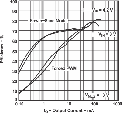 Figure 8-10 TPS65130 Efficiency vs Output Current
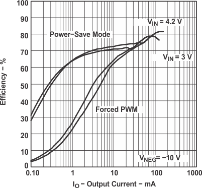 Figure 8-12 TPS65130 Efficiency vs Output Current
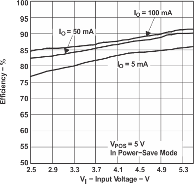 Figure 8-14 TPS65130 Efficiency vs Input Voltage
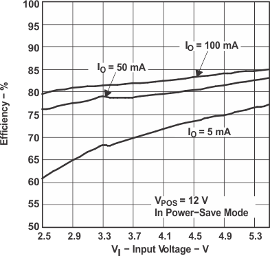 Figure 8-16 TPS65130 Efficiency vs Input Voltage
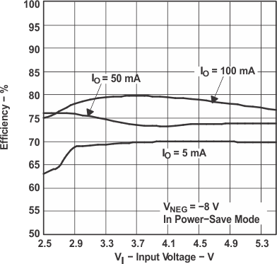 Figure 8-18 TPS65130 Efficiency vs Input Voltage
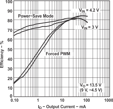 Figure 8-20 TPS65130 Combined Efficiency vs Output Current
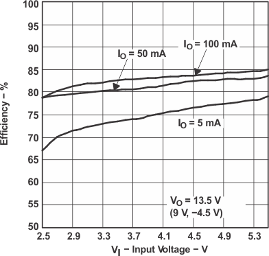 Figure 8-22 TPS65130 Combined Efficiency vs Input Voltage
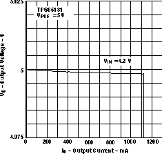 Figure 8-24 TPS65131 Output Voltage vs Output Current
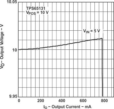 Figure 8-26 TPS65131 Output Voltage vs Output Current
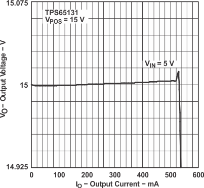 Figure 8-28 TPS65131 Output Voltage vs Output Current
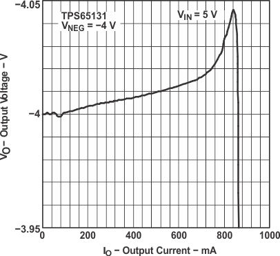 Figure 8-30 TPS65131 Output Voltage vs Output Current
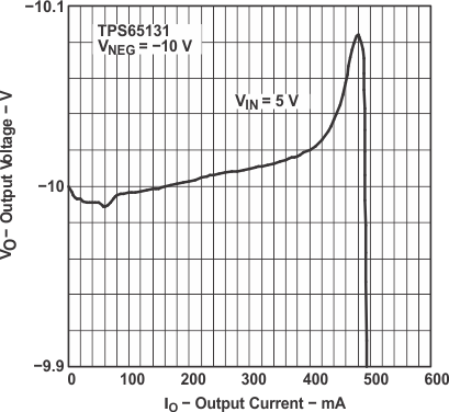 Figure 8-32 TPS65131 Output Voltage vs Output Current
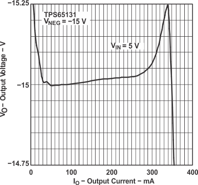 Figure 8-34 TPS65131 Output Voltage vs Output Current
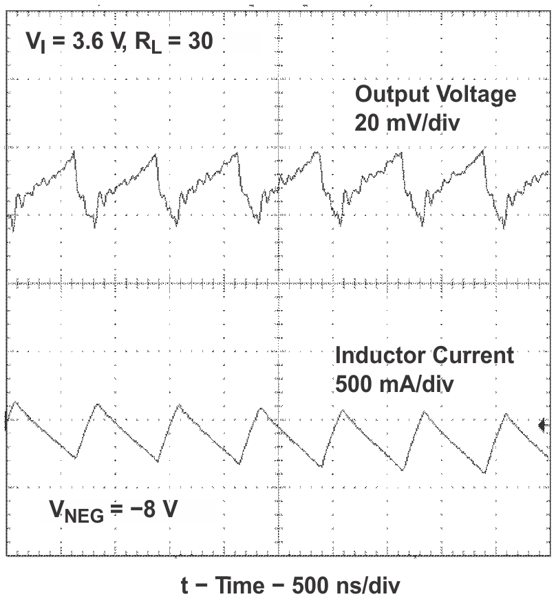 Figure 8-36 VNEG in Continuous Current Mode
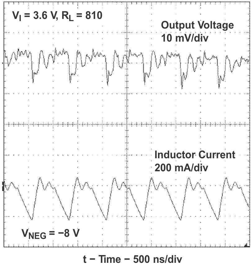 Figure 8-38 VNEG at Power-Save Mode Disabled
Figure 8-40 VNEG in Power-Save Mode
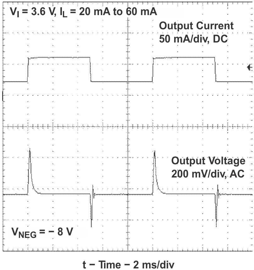 Figure 8-42 Load
Transient Response
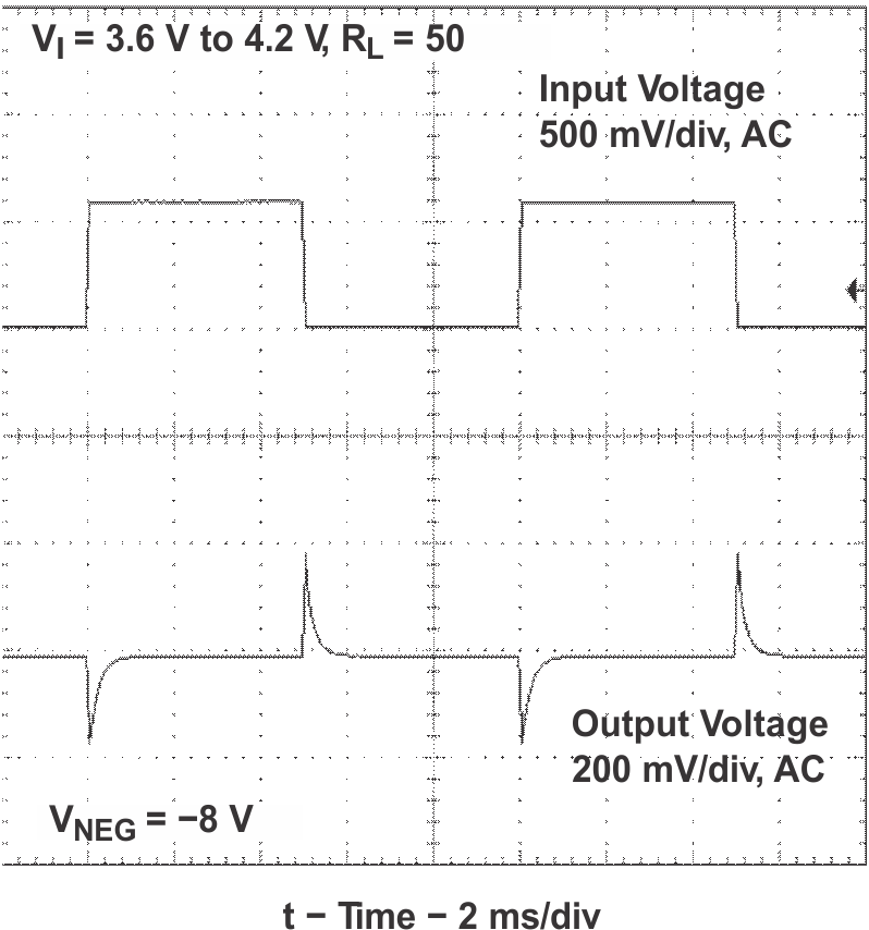 Figure 8-44 Line
Transient Response
Figure 8-44 Line
Transient ResponseFigure 8-46 Start-up After Enable
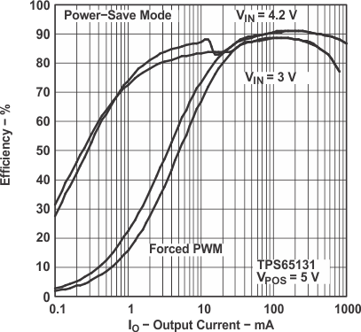 Figure 8-3 TPS65131 Efficiency vs Output Current
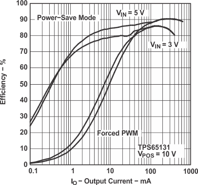 Figure 8-5 TPS65131 Efficiency vs Output Current
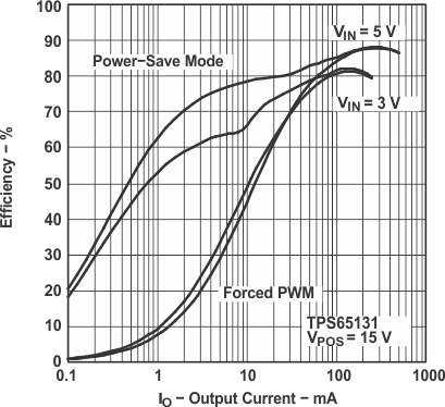 Figure 8-7 TPS65131 Efficiency vs Output Current
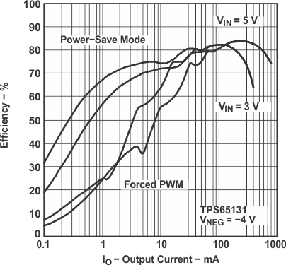 Figure 8-9 TPS65131 Efficiency vs Output Current
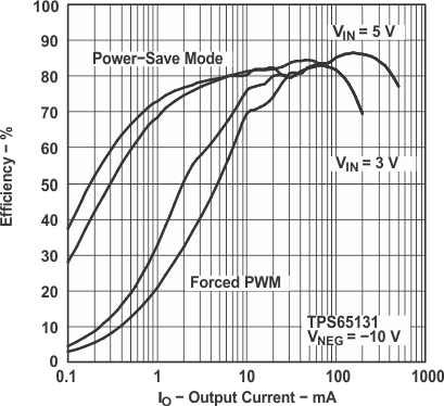 Figure 8-11 TPS65131 Efficiency vs Output Current
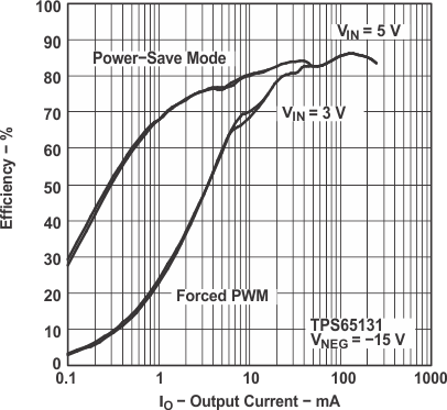 Figure 8-13 TPS65131 Efficiency vs Output Current
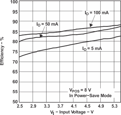 Figure 8-15 TPS65130 Efficiency vs Input Voltage
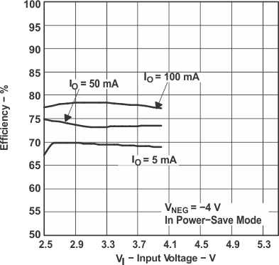 Figure 8-17 TPS65130 Efficiency vs Input Voltage
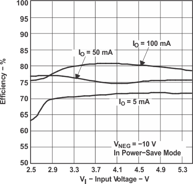 Figure 8-19 TPS65130 Efficiency vs Input Voltage
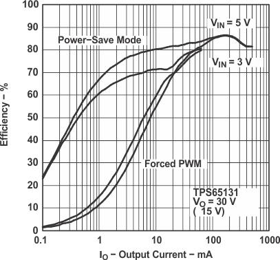 Figure 8-21 TPS65131 Combined Efficiency vs Output Current
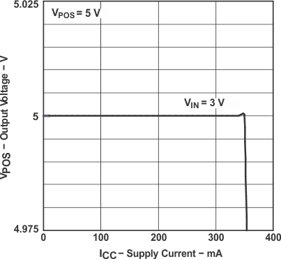 Figure 8-23 TPS65130 Output Voltage vs Output Current
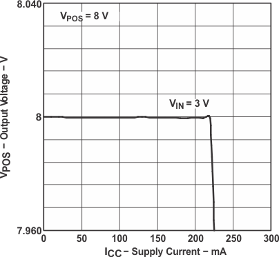 Figure 8-25 TPS65130 Output Voltage vs Output Current
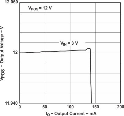 Figure 8-27 TPS65130 Output Voltage vs Output Current
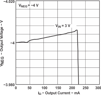 Figure 8-29 TPS65130 Output Voltage vs Output Current
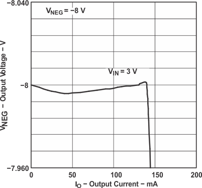 Figure 8-31 TPS65130 Output Voltage vs Output Current
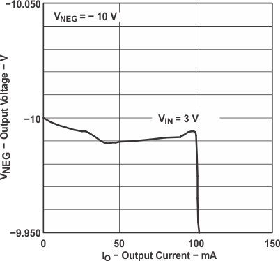 Figure 8-33 TPS65130 Output Voltage vs Output Current
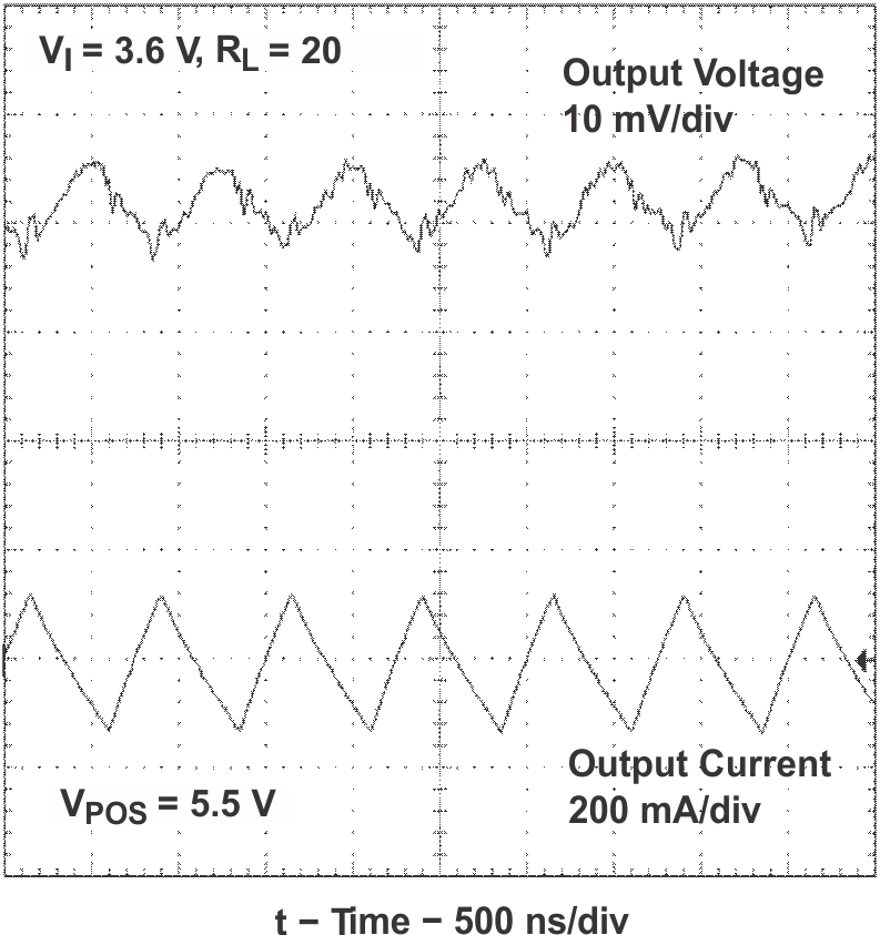 Figure 8-35 VPOS in Continuous Current Mode
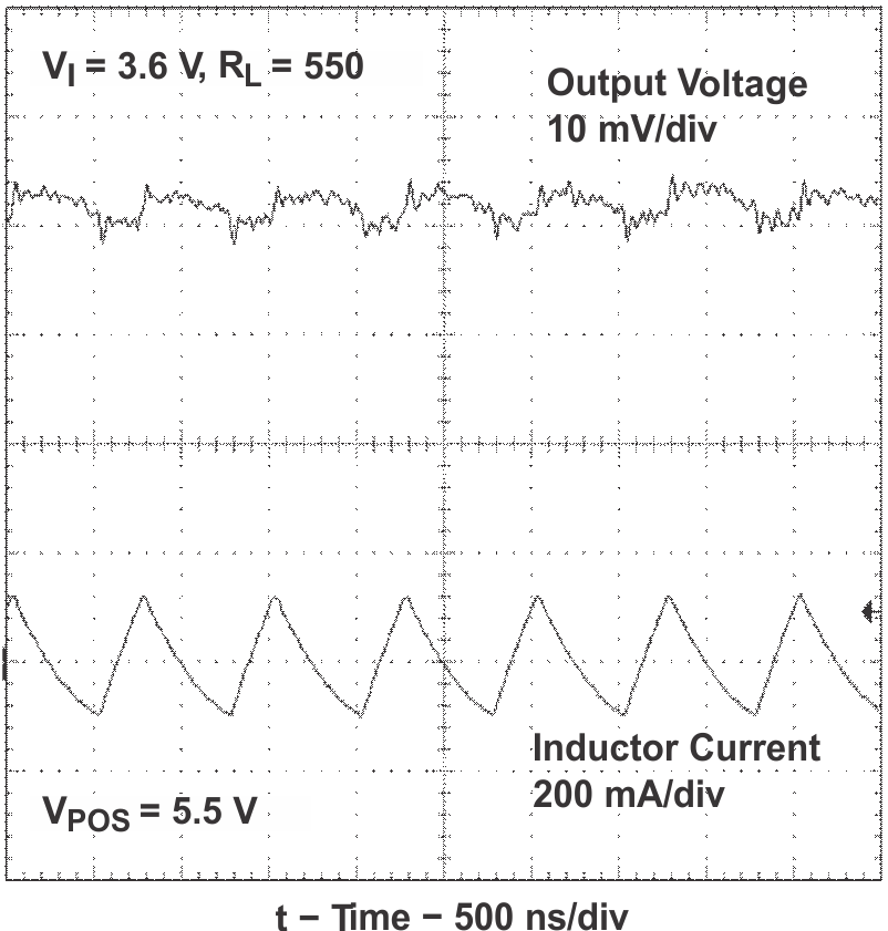 Figure 8-37 VPOS at Power-Save Mode Disabled
Figure 8-39 VPOS in Power-Save Mode
Figure 8-41 Load
Transient Response
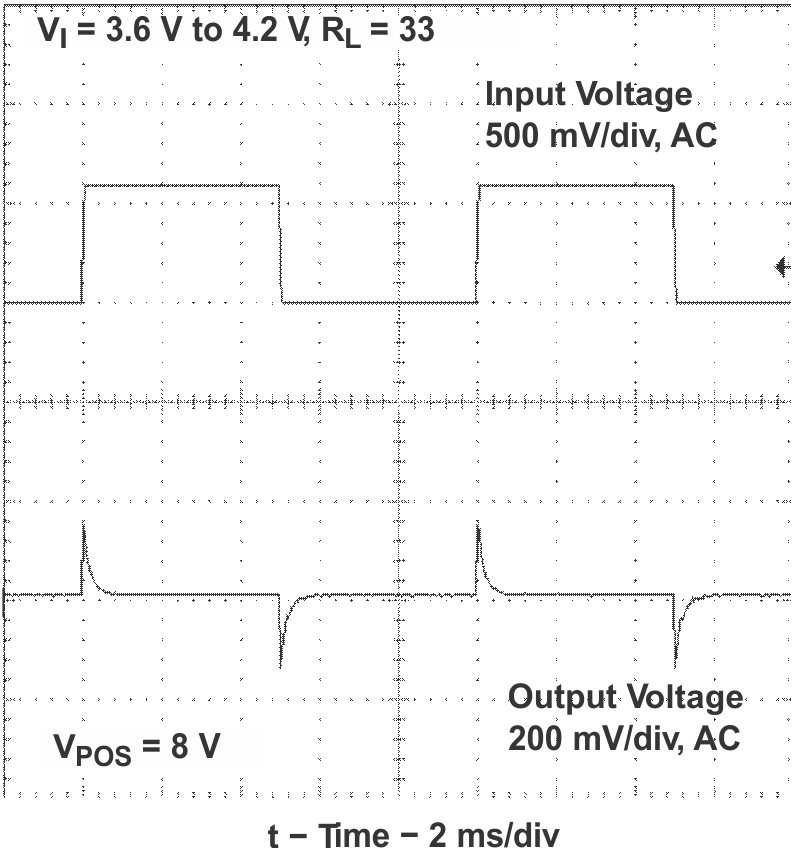 Figure 8-43 Line
Transient Response
Figure 8-43 Line
Transient ResponseFigure 8-45 Start-up After Enable