ZHCSCH4H June 2013 – November 2016 TPS65132
UNLESS OTHERWISE NOTED, this document contains PRODUCTION DATA.
- 1 特性
- 2 应用范围
- 3 说明
- 4 修订历史记录
- 5 Device Comparison Table
- 6 Pin Configuration and Functions
- 7 Specifications
- 8 Detailed Description
-
9 Application and Implementation
- 9.1 Application Information
- 9.2
Typical Applications
- 9.2.1
Low-current Applications (≤ 40 mA)
- 9.2.1.1 Design Requirements
- 9.2.1.2 Detailed Design Procedure
- 9.2.1.3 Application Curves
- 9.2.2
Mid-current Applications (≤ 80 mA)
- 9.2.2.1 Design Requirements
- 9.2.2.2 Detailed Design Procedure
- 9.2.2.3 Application Curves
- 9.2.3 High-current Applications (≤ 150 mA)
- 9.2.1
Low-current Applications (≤ 40 mA)
- 10Power Supply Recommendations
- 11Layout
- 12器件和文档支持
- 13机械、封装和可订购信息
8 Detailed Description
8.1 Overview
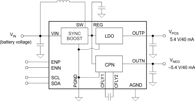
The TPS65132, supporting input voltage range from 2.5 V to 5.5 V, operates with a single inductor scheme to provide a high efficiency with a small solution size. The synchronous boost converter generates a positive voltage that is regulated down by an integrated LDO, providing the positive supply rail (VPOS). The negative supply rail (VNEG) is generated by an integrated negative charge pump (or CPN) driven from the boost converter output pin, REG. The operating mode can be selected between 40mA and 80mA in order to select the necessary output current capability and to get the best efficiency possible based on the application. The device topology allows a 100% asymmetry of the output currents.
8.2 Functional Block Diagram
8.3 Feature Description
8.3.1 Undervoltage Lockout (UVLO)
The TPS65132 integrates an undervoltage lockout block (UVLO) that enables the device once the voltage on the VIN pin exceeds the UVLO threshold (2.5 V maximum). No output voltage will be generated as long as the enable signals are not pulled HIGH. The device, as well as all converters (boost converter, LDO, CPN), will be disabled as soon as the VIN voltage falls below the UVLO threshold. The UVLO threshold is designed in a way that the TPS65132 will continue operating as long as VIN stays above 2.3 V. This guarantees a proper operation even in the event of extensive line transients when the battery gets suddenly heavily loaded.
For TPS65132Ax, a 40 ms delay is starting as soon as the UVLO threshold is reached. This delay prevents the device to be disabled and enabled by an unwanted VIN voltage spike. Once this delay has passed, the output rails can be enabled and disabled as desired with the enable signals without any delay.
8.3.2 Active Discharge
An active discharge of the positive rail and/or the negative rail can be programmed (DISP and DISN bits respectively - refer to Registers). If programmed to be active, the discharge will occur at power down, when the enable signals go LOW (Figure 37 and Figure 38 for TPS65132Ax, Bx, Lx, Tx, Wx — Figure 105 and Figure 104 for TPS65132Sx). See Power-Down And Discharge (LDO) and Power-Down And Discharge (CPN) for a detailed description of how each device variant implements the active discharge function.
8.3.3 Boost Converter
8.3.3.1 Boost Converter Operation
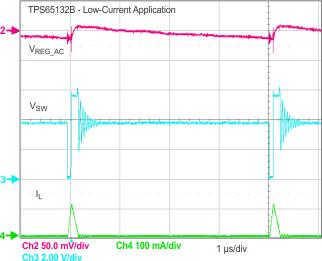
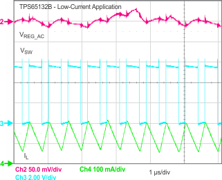
The synchronous boost converter uses a current mode topology and operates at a quasi-fixed frequency of typically 1.8 MHz, allowing chip inductors such as 2.2 µH or 4.7 µH to be used. The converter is internally compensated and provides a regulated output voltage automatically adjusted depending on the programmed VPOS and VNEG voltages. The boost converter operates either in continuous conduction mode (CCM) or Pulse Frequency Modulation mode (PFM), depending on the load current in order to provide the highest efficiency possible. The switch node waveforms for CCM and DCM operation are shown in Figure 6 and Figure 7.
8.3.3.2 Power-Up And Soft-Start (Boost Converter)
The boost converter starts switching as soon as one enable signal is pulled HIGH and the voltage on VIN pin is above the UVLO threshold. For TPS65132Ax, in the case where one enable signal is already HIGH when VIN reaches the UVLO threshold, the boost converter will only start switching after a 40 ms delay has passed (see Undervoltage Lockout (UVLO)).
The boost converter starts up with an integrated soft-start to avoid drawing excessive inrush current from the supply. The output voltage VREG is slowly ramped up to its target value. Typical startup waveforms for low-current applications are shown in Figure 33 and Figure 35.
8.3.3.3 Power-Down (Boost Converter)
The boost converter stops switching when VIN is below the UVLO threshold or when both output rails are disabled. For example, due to a special sequencing, the LDO might still be operating while the CPN is already disabled, in which case, the boost will continue operating until the LDO has been disabled. Typical power-down waveforms for low-current applications are shown in Figure 34 and Figure 36.
8.3.3.4 Isolation (Boost Converter)
The boost converter output (REG) is isolated from the input supply VIN, providing a true shutdown.
8.3.3.5 Output Voltage (Boost Converter)
The output voltage of the boost converter is automatically adjusted depending on the programmed VPOS and VNEG voltages.
8.3.3.6 Advanced Power-Save Mode For Light-Load Efficiency And PFM
The TPS65132 device integrates a power save mode to improve efficiency at light load. In power save mode the converter stops switching when the inductor current reaches 0 A. The device resumes its switching activity with one or more pulses once the VREG voltage falls below its regulation level, and goes again into power save mode once the inductor current reaches 0 A. The pulse duration remains constant, but the frequency of these pulses varies according to the output load. This operating mode is also known as Pulse Frequency Modulation or PFM. Figure 6 provides plots of the inductor current and the switch node in PFM mode.
8.3.4 LDO Regulator
8.3.4.1 LDO Operation
The Low Dropout regulator (or LDO) generates the positive voltage rail, VPOS, by regulating down the output voltage of the boost converter (VREG). Its inherent power supply rejection helps filtering the output ripple of the boost converter in order to provide on OUTP pin a clean voltage, e.g. to supply the source driver IC of the display.
8.3.4.2 Power-Up And Soft-Start (LDO)
The LDO starts operating as soon as the ENP signal is pulled HIGH, VIN voltage is above the UVLO threshold and the boost converter has reached its Power Good threshold.
In the case where the enable signal is already HIGH when VIN exceeds the UVLO threshold, the boost converter will start first and the LDO will only start after the boost converter has reached its target voltage. For TPS65132Ax, the boost will start after the 40 ms delay has passed (see Undervoltage Lockout (UVLO)).
For TPS65132Sx the LDO startup is defined by the setting of the DLYx register and the SEQU bits, see Registers for more details.
The LDO integrates a soft-start that slowly ramps up its output voltage VPOS regardless of the output capacitor and the target voltage, as long as the LDO current limit is not reached. For TPS65132Ax and TPS65132Bx (except TPS65132B2), the typical startup time is 140 µs. For TPS65132B2, TPS65132Lx, TPS65132Sx, TPS65132Tx and TPS65132Wx, the typical ramp-up time is 500 µs and the inrush current is also reduced by a factor of 3. Typical startup waveforms for the low-current application are shown in Figure 33 to Figure 35.
8.3.4.3 Power-Down And Discharge (LDO)
The LDO stops operating when VIN is below the UVLO threshold or when ENP is pulled LOW. Or for TPS65132Sx when EN is pulled LOW, and the internal sequencing has passed.
The positive rail can be actively discharged to GND during power-down if required. A discharge selection bit is available to enable or disable this function. See Registers for more details, as well as waveforms in Figure 37 and Figure 38. Table 1 shows the VPOS active discharge behavior of each device variant.
Table 1. VPOS Active Discharge Behavior
| PART NUMBER | VIN | ENP (or EN) | ENN (or SYNC) | VPOS DISCHARGE |
|---|---|---|---|---|
| TPS65132Ax | < VUVLO | Don't Care | Don't Care | On |
| > VUVLO | Low | Low | Determined by DISP bit | |
| Low | High | Determined by DISP bit | ||
| High | Low | Off | ||
| High | High | Off | ||
| TPS65132Bx TPS65132Lx TPS65132Sx TPS65132Tx TPS65132Wx |
< VUVLO | Don't Care | Don't Care | On |
| > VUVLO | Low | Low | On | |
| Low | High | Determined by DISP bit | ||
| High | Low | Off | ||
| High | High | Off |
8.3.4.4 Isolation (LDO)
The LDO is isolating the VPOS rail from VREG (boost converter output) as long as the rail is not enabled in order to ensure flexible startup like VNEG before VPOS.
8.3.4.5 Setting The Output Voltage (LDO)
The output voltage of the LDO is programmable via a I2C compatible interface, from –6.0 V to –4.0 V in 100 mV steps. For more details, please refer to the VPOS Register – Address: 0x00
8.3.5 Negative Charge Pump
8.3.5.1 Operation
The negative charge pump (CPN) generates the negative voltage rail, VNEG, by inverting and regulating the output voltage of the boost converter (VREG). The charge pump uses 4 switches and an external flying capacitor to generate the negative rail. Two of the switches are turned on in the first phase to charge the flying capacitor up to VREG, and in the second phase they are turned-off and the two others turn on to pump the energy negatively out of the OUTN capacitor.
8.3.5.2 Power-Up And Soft-Start (CPN)
The CPN starts operating as soon as the ENN signal is pulled HIGH, VIN voltage is above the UVLO threshold and the boost converter has reached its Power Good threshold.
In the case where the enable signal is already HIGH when VIN reaches the UVLO threshold, the boost converter will start first and the CPN will only start after the boost converter has reached its target voltage. For TPS65132Ax, the boost will start after the 40 ms delay has passed (see Undervoltage Lockout (UVLO)).
For TPS65132Sx the CPN startup is defined by the setting of the DLYx register and the SEQU bits, see Registers for more details.
The CPN integrates a soft-start that slowly ramps up its output voltage VNEG within a time defined by the selected mode (40mA or 80mA), the output voltage and the output capacitor value. For TPS65132Ax and TPS65132Bx (except TPS65132B2), the startup current charging the output capacitor in 40mA mode is 50 mA, and 100 mA typically in 80mA mode. For TPS65132B2, TPS65132Lx, TPS65132Tx, and TPS65132Wx, the typical ramp-up times are slowed down by a factor of 4 (i.e 12.5 mA and 25 mA typical output current for 40mA and 80mA modes respectively) and the inrush current is also reduced by a factor of about 4. Typical startup waveforms for the low-current application are shown in Figure 39 to Figure 42.
For TPS65132Sx, the negative rail starts-up in 40mA or 80mA mode, thus the startup current is set by the mode the device is programmed to, and not related to the SYNC pin state. The full current of 150 mA minimum is only released once both rails (VPOS and VNEG) have reached their Power Good levels.
The estimated startup time can be calculated using the following formula: 
Where:
tSTARTUP = startup time of the VNEG rail
COUT = output capacitance of the VNEG rail
VNEG = target output voltage
ISTARTUP = output current of the VNEG rail charging up the output capacitor at startup (12.5 mA, 25 mA, 50 mA or 100 mA as described above)
8.3.5.3 Power-Down And Discharge (CPN)
The CPN stops operating when VIN is below the UVLO threshold or when ENN is pulled LOW.
Or when EN is pulled LOW in the TPS65132Sx, and the internal sequencing has passed.
The negative rail can be actively discharged to GND during power-down if required. A discharge selection bit is available to enable or disable this function. See for more details, as well as waveforms Figure 37 and Figure 38. Table 2 shows the VNEG discharge behavior of each device variant.
Table 2. VNEG Active Discharge Behavior
| PART NUMBER | VIN | ENP (or EN) | ENN (or SYNC) | VNEG DISCHARGE |
|---|---|---|---|---|
| TPS65132Ax | < VUVLO | Don't Care | Don't Care | On |
| > VUVLO | Low | Low | Determined by DISN bit | |
| Low | High | Off | ||
| High | Low | Determined by DISN bit | ||
| High | High | Off | ||
| TPS65132Bx TPS65132Lx TPS65132Tx TPS65132Wx |
< VUVLO | Don't Care | Don't Care | On |
| > VUVLO | Low | Low | On | |
| Low | High | Off | ||
| High | Low | Determined by DISN bit | ||
| High | High | Off | ||
| TPS65132Sx | < VUVLO | Don't Care | Don't Care | On |
| > VUVLO | Low | Low | On | |
| Low | High | Determined by DISN bit | ||
| High | Low | Off | ||
| High | High | Off |
8.3.5.4 Isolation (CPN)
The CPN isolates the VNEG rail from VREG (boost converter output) as long as the rail is not enabled in order to ensure flexible startup like VPOS before VNEG.
8.3.5.5 Setting The Output Voltage (CPN)
The output voltage of the CPN is programmable via a I2C compatible interface, from –4.0 V to –6.0 V in 100 mV steps. For more details, please refer to the VNEG Register – Address 0x01.
8.4 Device Functional Modes
8.4.1 Enabling and Disabling the Device
At startup (VIN goes above UVLO and at least one of the enable pins (ENP, ENN, or EN) goes HIGH), the EEPROM content is loaded into the DAC registers and the IC starts with these default values. The TPS65132 is enabled as long as the VIN voltage is above the UVLO and one of the enable pins (ENP, ENN, or EN) is HIGH.
Pulling ENP or ENN LOW disables either rail (VPOS or VNEG respectively); and, pulling both pins LOW disables the device entirely (the internal oscillator of the TPS65132Ax continues running to allow access to the I²C interface).
For TPS65132Sx, pulling EN LOW disables the device.
8.5 Programming
8.5.1 I2C Serial Interface Description
The TPS65132 communicates through an industry standard I2C compatible interface, to receive data in slave mode. I2C is a 2-wire serial interface developed by Philips Semiconductor (see I2C-Bus Specification, Version 2.1, January 2000).
The TPS65132 integrates a non-volatile memory (EEPROM) that allows the storage of the register values with a capability of up to 1000 programming cycles. At startup the TPS65132 loads first the EEPROM content into the registers and uses these voltages to start.
It is recommended to stop I2C communication with the TPS65132 for 50 ms after the command "Write EEPROM data" was sent. If the device is accessed via I2C during EEPROM programming, the device will pull down the SCL line (clock stretch) after it recognized its I2C address. The SCL line will be released after EEPROM programming is finished.
The TPS65132 works as a slave and supports the following data transfer modes, as defined in the I2C-Bus specification: standard mode (100 kbps) and fast mode (400 kbps). The data transfer protocol for standard and fast modes is exactly the same, therefore they are referred to as F/S-mode in this document. The TPS65132 supports 7-bit addressing. The device 7-bit address is 3E (see Figure 8), and the LSB enables the write or read function.
| MSB | TPS65132 | Address | LSB | ||||
| 0 | 1 | 1 | 1 | 1 | 1 | 0 | R/W |
| R/W = R/(W) | |||||||
NOTE
With TPS65132Ax, the I2C interface is accessible as long as the input voltage is above the undervoltage lockout threshold. In all other versions, the I2C interface is accessible only as soon as one of the enable pins is pulled HIGH while the input voltage is above the undervoltage lockout.
8.5.2 I2C Interface Protocol
 Figure 9. “Write" Data To DAC – Transfer Format In F/S-Mode
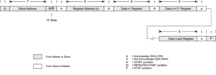 Figure 10. "Write" Data To DAC – Transfer Format In F/S-Mode
 Featuring Register Address Auto-Increment
 Figure 11. “Write” Data To EEPROM – Transfer Format In F/S-Mode
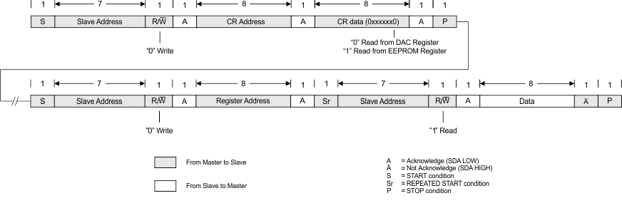 Figure 12. “Read” Data From DAC/EEPROM – Transfer Format In F/S-Mode
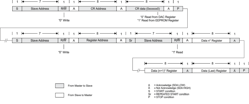 Figure 13. “Read” Data From DAC/EEPROM – Transfer Format In F/S-Mode
 Featuring Register Address Auto-Increment
8.6 Register Maps
The TPS65132 has a non-volatile memory (EEPROM) which contains the initial values and one volatile memory (Registers) which contains the actual settings. The EEPROM and the Registers are accessed with the same address.
Startup option: At power-up, the values contained in the EEPROM are loaded into the Registers to the last stored setting within less than 20 µs. The programmed factory value of the EEPROM of each address is described in section Factory Default Register Value.
Write description: The user has to program all Registers first (0×00 to 0×03), then set the WED (Write EEPROM Data) bit to 1. A dead time of 50 ms is then initiated during which the register content or all registers (0×00 ~ 0×03) are stored into the non-volatile EEPROM cells. During that time, there should be no data flowing through the I2C because the I2C interface is momentarily not responding.
After the 50 ms have passed, the WED bit is automatically reset to 0, and the user is able to read the values or program again.
| Slave address: | 0x3E |
| X = R/W | R/W = 1 → read mode |
| R/W = 0 → write mode |
8.6.1 Registers
Attempting to read data from register addresses not listed in the following section will result in 0x00 being read out.
8.6.1.1 VPOS Register – Address: 0x00
| 7 | 6 | 5 | 4 | 3 | 2 | 1 | 0 |
| RSVD | RSVD | RSVD | VPOS[4:0] | ||||
| 0 | 0 | 0 | 0 | 1 | 1 | 1 | 0 |
| R | R/W | ||||||
| LEGEND: R/W = Read/Write; R = Read only; -n = value after reset |
Table 3. VPOS Register Field Descriptions
| Bit | Field | Description | |||
|---|---|---|---|---|---|
| 7:5 | RSVD[2:0] | Reserved, always set to 0 | |||
| 4:0 | VPOS[4:0] | VPOS output voltage adjustment | |||
| VPOS[4:0] Value (binary) | VPOS Output Voltage (V) | VPOS[4:0] Value (binary) | VPOS Output Voltage (V) | ||
| 00000 | 4.0 | 01011 | 5.1 | ||
| 00001 | 4.1 | 01100 | 5.2 | ||
| 00010 | 4.2 | 01101 | 5.3 | ||
| 00011 | 4.3 | 01110 | 5.4 | ||
| 00100 | 4.4 | 01111 | 5.5 | ||
| 00101 | 4.5 | 10000 | 5.6 | ||
| 00110 | 4.6 | 10001 | 5.7 | ||
| 00111 | 4.7 | 10010 | 5.8 | ||
| 01000 | 4.8 | 10011 | 5.9 | ||
| 01001 | 4.9 | 10100 | 6.0 | ||
| 01010 | 5.0 | ||||
8.6.1.2 VNEG Register – Address 0x01
| 7 | 6 | 5 | 4 | 3 | 2 | 1 | 0 |
| RSVD | RSVD | RSVD | VNEG[4:0] | ||||
| 0 | 0 | 0 | 0 | 1 | 1 | 1 | 0 |
| R | R/W | ||||||
| LEGEND: R/W = Read/Write; R = Read only; -n = value after reset |
Table 4. VNEG Register Field Descriptions
| Bit | Field | Description | |||
|---|---|---|---|---|---|
| 7:5 | RSVD[2:0] | Reserved, always set to 0 | |||
| 4:0 | VNEG[4:0] | VNEG output voltage adjustment | |||
| VNEG[4:0] Value (binary) | VNEG Output Voltage (V) | VNEG[4:0] Value (binary) | VNEG Output Voltage (V) | ||
| 00000 | –4.0 | 01011 | –5.1 | ||
| 00001 | –4.1 | 01100 | –5.2 | ||
| 00010 | –4.2 | 01101 | –5.3 | ||
| 00011 | –4.3 | 01110 | –5.4 | ||
| 00100 | –4.4 | 01111 | –5.5 | ||
| 00101 | –4.5 | 10000 | –5.6 | ||
| 00110 | –4.6 | 10001 | –5.7 | ||
| 00111 | –4.7 | 10010 | –5.8 | ||
| 01000 | –4.8 | 10011 | –5.9 | ||
| 01001 | –4.9 | 10100 | –6.0 | ||
| 01010 | –5.0 | ||||
8.6.1.3 DLYx Register – Address 0x02 (Only valid for TPS65132Sx)
| 7 | 6 | 5 | 4 | 3 | 2 | 1 | 0 |
| DLYP2 | DLYP2 | DLYN2 | DLYN2 | DLYP1 | DLYP1 | DLYN1 | DLYN1 |
| 0 | 0 | 0 | 0 | 0 | 0 | 0 | 1 |
| R/W | |||||||
Table 5. DLYx Register Field Descriptions
| Bit | Field | Description | |||
|---|---|---|---|---|---|
| 7:6 | DLYP2[1:0] | Delay in milliseconds | |||
| 5:4 | DLYN2[1:0] | ||||
| 3:2 | DLYP1[1:0] | ||||
| 1:0 | DLYN1[1:0] | ||||
| DLYx[1:0] | DLYx Value (binary) | DLYx Delay (ms) | |||
| 00 | 0 | ||||
| 01 | 1 | ||||
| 10 | 5 | ||||
| 11 | 10 | ||||
8.6.1.4 APPS - SEQU - SEQD - DISP - DISN Register – Address 0x03
| 7 | 6 | 5 | 4 | 3 | 2 | 1 | 0 |
| RSVD | APPS | SEQU | SEQU | SEQD | SEQD | DISP | DISN |
| 0 | 0 | 0 | 0 | 0 | 0 | 1 | 0 |
| R | R/W | R/W | R/W | R/W | R/W | R/W | R/W |
| LEGEND: R/W = Read/Write; R = Read only; -n = value after reset |
Table 6. APPS - SEQU - SEQD - DISP - DISN Field Descriptions
| Bit | Field | Description | Value (binary) | Action | ||
|---|---|---|---|---|---|---|
| 7 | RSVD | Reserved, always set to 0 | ||||
| 6 | APPS | Application | APPS Value | 0 | 40mA | |
| 1 | 80mA | |||||
| 5:4 | SEQU(1) | Sequencing at Startup | SEQU Value | 00 | VPOS and VNEG simultaneously (DLYP1 after EN goes HIGH) | |
| 01 | VPOS (DLYP1 after EN goes HIGH) and then VNEG (DLYN1 after VPOS) | |||||
| 10 | VNEG (DLYN1 after EN goes HIGH) and then VPOS (DLYP1 after VNEG) | |||||
| 11 | VPOS only | |||||
| 3:2 | SEQD(1) | Sequencing at Shutdown | SEQD Value | 00 | VPOS and VNEG simultaneously (DLYP2 after EN goes LOW) | |
| 01 | VPOS (DLYP2 after EN goes LOW) and then VNEG (DLYN2 after VPOS) | |||||
| 10 | VNEG (DLYN2 after EN goes LOW) and then VPOS (DLYP2 after VNEG) | |||||
| 11 | Ignored | |||||
| 1 | DISP(2) | Discharge VPOS | DISP Value | 0 | No discharge | |
| 1 | VPOS actively discharged | |||||
| 0 | DISN(2) | Discharge VNEG | DISN Value | 0 | No discharge | |
| 1 | VNEG actively discharged | |||||
8.6.1.5 Control Register – Address 0xFF
| 7 | 6 | 5 | 4 | 3 | 2 | 1 | 0 |
| WED | RSVD[6:1] | EE/(DR) | |||||
| The Reserved bits are ignored when written and return either 0 or 1 when read. |
Table 7. Control Register Field Descriptions
| Bit | Field | Value (binary) | Description | |||
|---|---|---|---|---|---|---|
| 7 | WED | 0 | No action | |||
| 1 | Write EEPROM Data | |||||
| 6:1 | RSVD[6:1] | Reserved | ||||
| 0 | EE/(DR) | 0 | Read from Registers | |||
| 1 | Read from EEPROM | |||||
8.6.2 Factory Default Register Value
| Part number | Register address | ||||
|---|---|---|---|---|---|
| 0x00 | 0x01 | 0x02 | 0x03 | ||
| TPS65132A | 0x0E | 0x0E | — | 0x03 | |
| TPS65132A0 | 0x0A | 0x0A | — | 0x03 | |
| TPS65132B | 0x0E | 0x0E | — | 0x03 | |
| TPS65132B0 | 0x0A | 0x0A | — | 0x03 | |
| TPS65132B2 | 0x0C | 0x0C | — | 0x03 | |
| TPS65132B5 | 0x0F | 0x0F | — | 0x03 | |
| TPS65132L | 0x0E | 0x0E | — | 0x03 | |
| TPS65132L0 | 0x0A | 0x0A | — | 0x03 | |
| TPS65132L1 (1) | 0x0B | 0x0B | — | 0x03 | |
| TPS65132S | 0x0E | 0x0E | 0x00 | 0x43 | |
| TPS65132T6 | 0x10h | 0x10h | — | 0x43 | |
| TPS65132W | 0x0E | 0x0E | — | 0x43 | |
