ZHCS495C November 2011 – January 2017 TPS65135
PRODUCTION DATA.
10 Layout
10.1 Layout Guidelines
No PCB layout is perfect, and compromises are always necessary. However, the basic principles listed below (in order of importance) go a long way to achieving the full performance of the TPS65135 device.
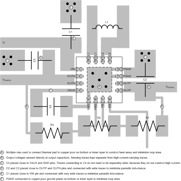
- If possible, route discontinuous switching currents on the top layer, using short, wide traces to minimize stray inductance and resistance. For the TPS65135 device, the current flowing into the VIN, L1, L2, VPOS, VNEG and PGND pins is discontinuous. In the example layout below, vias are used to connect discontinuous return currents to the ground plane, as it is considered a slightly better approach with this device than forcing all currents to flow on the top layer.
- Place C1 and C4 as close as possible to the VIN and AVIN pins respectively.
- Place C2 and C3 as close as possible to the VPOS and VNEG pins respectively.
- Place L1 as close as possible to the L1 and L2 pins.
- Use a copper pour (preferably on layer 2) as a thermal spreader and connect it to the exposed thermal pad using the maximum number of thermal vias (see packaging information for more information on the recommended thermal vias).
- The copper pour described above can be used as a ground plane if it is not possible to route power ground signals on the top layer.
10.2 Layout Example
Figure 27 shows an example PCB layout based on the above principles.
 Figure 27. PCB Layout Example