ZHCS495C November 2011 – January 2017 TPS65135
PRODUCTION DATA.
8 Application and Implementation
NOTE
Information in the following applications sections is not part of the TI component specification, and TI does not warrant its accuracy or completeness. TI’s customers are responsible for determining suitability of components for their purposes. Customers should validate and test their design implementation to confirm system functionality.
8.1 Application Information
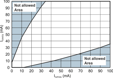
The TPS65135 device can be used to generate spilt-rail supplies from input supply voltages in the range 2.5 V to 5.5 V and has been optimized for use with 3.3-V rails of single-cell Li-ion batteries. It can generate positive output voltages up to 6 V and negative voltages down to –7 V with buck-boost action (i.e. the input supply voltage may be above or below the positive output voltage), as long as the output current mis-match is 50% or less. Both outputs are controlled by the EN pin: a high logic level enables both outputs, and a low logic level disables them. An integrated UVLO function disables the device when the input supply voltage is too low for proper operation.
8.2 Typical Application
Figure 8 shows a typical application for a ±5-V AMOLED display supply.
SPACE
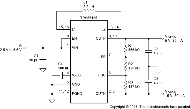 Figure 8. Standard Application ±5-V Supply
8.2.1 Design Requirements
Table 2 shows the design requirements for a ±5-V AMOLED supply application used as an example to illustrate the design process.
Table 2. Design Parameters
| PARAMETER | SYMBOL | EXAMPLE VALUE |
|---|---|---|
| Input Supply Voltage Range | VI | 2.5 V to 5.5 V |
| Positive Output Voltage | VO(POS) | 5 V |
| Negative Output Voltage | VO(NEG) | –5 V |
| Maximum Positive Output Current | IO(POS) max | 80 mA |
| Maximum Negative Output Current | IO(NEG) max | –80 mA |
8.2.2 Detailed Design Procedure
8.2.2.1 Choosing a Suitable Inductor
The TPS65135 device is internally compensated and operates best with a 2.2-µH inductor. For this type of converter, selection of the inductor is a key element in the design process because it has a big impact on the efficiency, the line and load transient response, and the maximum output current the device is able to deliver. Because the inductor ripple current is fairly large in the SIMO topology, the inductor core losses largely determine converter efficiency. As a result, an inductor with a relatively large dc winding resistance (DCR) but low core losses can often achieve higher converter efficiencies than other inductors with lower DCR but higher core losses.
As previously described, the converter's line transient response is highest when the converter operates in DCM, and since larger inductor values cause the converter to enter CCM operation at lower load currents, smaller inductor values give the best line transient response. The formula to calculate the output current at which the converter enters CCM operation is shown in Equation 3. The inductors listed in Table 3 achieve a good overall converter efficiency while having a low height. The first two TOKO inductors achieve the highest efficiency (almost identical) followed by the LPS3008. The best compromise between efficiency and inductor size is given by the XFL2006 inductor. The inductor saturation current should typically be 1 A or higher, however, if the output current required by the application is low, inductors with smaller saturation current ratings may be considered.
Table 3. Inductor Selection
| INDUCTOR VALUE | COMPONENT SUPPLIER | DIMENSIONS in mm | Isat / DCR |
|---|---|---|---|
| 2.2 µH | TOKO DFE252010C | 2.5 x 2 x 1 | 1.9 A / 130 mΩ |
| TOKO DFE252012C | 2.5 x 2 x 1.2 | 2.2 A / 90 mΩ | |
| Coilcraft XFL2006-222 | 2 × 1.9 × 0.6 | 0.8 A / 278 mΩ | |
| Coilcraft LPS3008-222 | 3 × 3 × 0.8 | 1.1 A / 175 mΩ | |
| Samsung CIG2MW2R2NNE | 2 × 1.6 × 1 | 1.2 A / 110 mΩ | |
| TOKO FDSE0312-2R2 | 3.3 × 3.3 × 1.2 | 1.2 A / 160 mΩ | |
| ABCO LPF3010T-2R2 | 2.8 × 2.8 × 1 | 1.0 A / 100 mΩ | |
| Maruwa CXFU0208-2R2 | 2.65 × 2.65 × 0.8 | 0.85 A / 185 mΩ |
8.2.2.2 Choosing Suitable Input and Output Capacitors
The TPS65135 device typically requires a 10-µF ceramic input capacitor. Larger values can be used to lower the input voltage ripple. Table 4 lists capacitors suitable for use on the TPS65135 input.
Table 4. Input Capacitor Selection
| CAPACITOR | COMPONENT SUPPLIER | SIZE |
|---|---|---|
| 10 µF / 6.3V | Murata GRM188R60J106ME84D | 0603 |
| 10 µF / 6.3 V | Taiyo Yuden JMK107BJ106 | 0603 |
A 4.7-µF output capacitor is generally sufficient for most applications, but larger values can be used as well for improved load- and line-transient response at higher load currents. The capacitors of Table 5 have been found to work well with the TPS65135 device.
Table 5. Output Capacitor Selection
| CAPACITOR | COMPONENT SUPPLIER | SIZE |
|---|---|---|
| 10 µF / 6.3 V | Murata GRM188R60J106ME84D | 0603 |
| 4.7 µF / 10 V | Taiyo Yuden LMK107BJ475 | 0603 |
| 10 µF / 6.3 V | Taiyo Yuden JMK107BJ106 | 0603 |
8.2.2.3 Choosing Suitable Feedback Resistors
Equation 7 can be used to calculate a suitable value for R2, so that the recommended current of ≈10 µA flows through the feedback resistors.
The value of R1 can be calculated by rearranging Equation 7, so that
SPACE

SPACE
Inserting R2 = 120 kΩ, Vref1 = 1.24 V and VO(POS) = 5 V into Equation 10, we get
SPACE

SPACE
The closest 1%-tolerance standard value is 365 kΩ, which will generate a nominal output voltage of 5.012 V.
The value of R3 can be calculated by rearranging Equation 9, so that
SPACE

SPACE
Inserting R2 = 120 kΩ, Vref1 = 1.24 V and VO(NEG) = –5 V into Equation 12, we get
SPACE

SPACE
The closest 1%-tolerance standard value is 487 kΩ, which will generate a nominal output voltage of –5.032 V.
8.2.2.4 Measurement Circuit
The following application curves were obtained using the circuit shown in Figure 9 and the external components listed in Table 6.
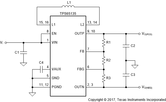 Figure 9. Measurement Circuit
Table 6. Component List
| Reference | Description | Manufacturer and Part Number |
|---|---|---|
| C1, C2, C3 | 10 μF, 6.3 V, 0603, X5R, ceramic | Murata, GRM188R60J106ME84D |
| C4 | 100 nF, 10 V, 0603, X7R, ceramic | Murata, GRM188R71H104KA93D |
| L1 | 2.2 μH, 2.2 A, 90 mΩ, 2.5 mm × 2.0 mm × 1.2 mm | Toko, 1239AS-H-2R2M |
| R1 | Depending on the output voltage, 1%, (all measurements with ±5 V output voltage uses 365 kΩ) | |
| R2 | Depending on the output voltage, 1%, (all measurements with ±5 V output voltage uses 120 kΩ) | |
| R3 | Depending on the output voltage, 1%, (all measurements with ±5 V output voltage uses 487 kΩ) | |
| U1 | TPS65135RTE | Texas Instruments |
8.2.3 Application Curves
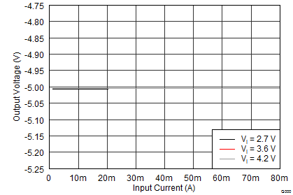
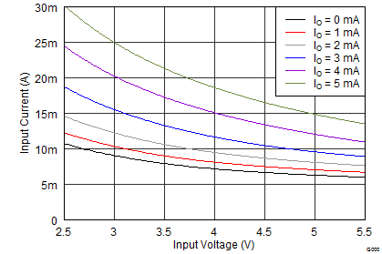
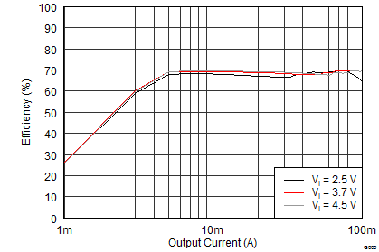
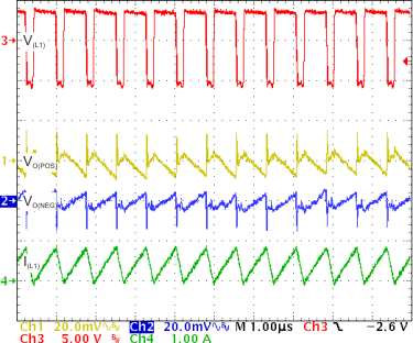
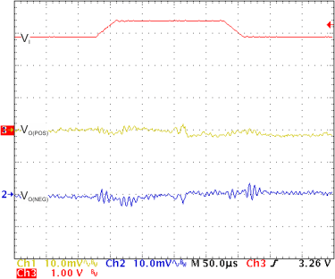
In the following curves VI = 3.7 V, VO(POS) = 5 V, VO(NEG) = –5 V unless otherwise noted. Where the symbol IO is used, it implies that IO(POS) = |IO(NEG)|. All measurements at TA = 25°C unless otherwise noted.
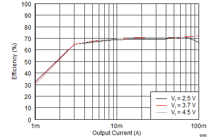
| L1 = 2.2 µH | ||
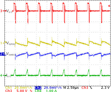
| IO = 10 mA | ||
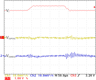
| IO = 10 mA | VI = 2.9 V, 3.4 V |
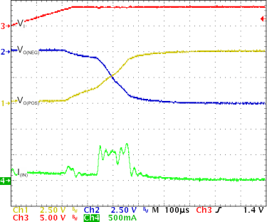
| IO = 0 mA | ||
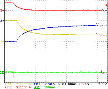
| IO = 0 mA | ||
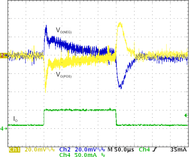
| IO = 10 mA, 50 mA | ||
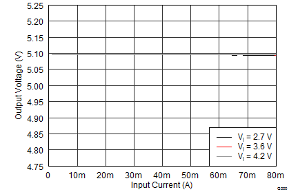
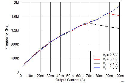
| L1 = 4.7 µH | ||
| IO = 80 mA | ||
| IO = 50 mA | VI = 2.9 V, 3.4 V |
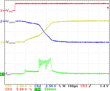
| IO = 0 mA | ||
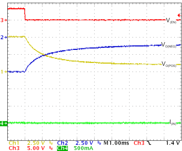
| IO = 0 mA | ||
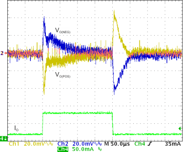
| IO = 20 mA, 80 mA | ||
