ZHCSBL3C June 2013 – May 2017 TPS65150-Q1
PRODUCTION DATA.
- 1 特性
- 2 应用
- 3 说明
- 4 修订历史记录
- 5 Pin Configuration and Functions
- 6 Specifications
- 7 Detailed Description
-
8 Application and Implementation
- 8.1 Application Information
- 8.2
Typical Application
- 8.2.1 Design Requirements
- 8.2.2
Detailed Design Procedure
- 8.2.2.1 Boost Converter Design Procedure
- 8.2.2.2 Rectifier Diode Selection
- 8.2.2.3 Setting the Output Voltage
- 8.2.2.4 Output Capacitor Selection
- 8.2.2.5 Input Capacitor Selection
- 8.2.2.6 Compensation
- 8.2.2.7 Negative Charge Pump
- 8.2.2.8 Positive Charge Pump
- 8.2.2.9 Gate Voltage Shaping
- 8.2.2.10 Power-On Sequencing
- 8.2.2.11 Fault Delay
- 8.2.3 Application Curves
- 8.3 System Examples
- 9 Power Supply Recommendations
- 10Layout
- 11器件和文档支持
- 12机械、封装和可订购信息
10 Layout
10.1 Layout Guidelines
The PCB layout is an important step in the power supply design. An incorrect layout could cause converter instability, load regulation problems, noise, and EMI issues. Especially with a switching DC-DC converter at high load currents, too-thin PCB traces can cause significant voltage spikes. Good grounding is also important. If possible, TI recommends using a common ground plane to minimize ground shifts between analog ground (GND) and power ground (PGND). Additionally, the following PCB design layout guidelines are recommended for the TPS65150-Q1 device:
- Boost converter output capacitor, input capacitor and Power ground (PGND) must form a star ground or must be directly connected together on a common power ground plane.
- Place the input capacitor directly from the input pin (VIN) to ground.
- Use a bold PCB trace to connect SUP to the output Vs.
- Place a small bypass capacitor from the SUP pin to ground.
- Use short traces for the charge-pump drive pins (DRVN, DRVP) of VGH and VGL because these traces carry switching currents.
- Place the charge pump flying capacitors as close as possible to the DRVP and DRVN pin, avoiding a high voltage spikes at these pins.
- Place the Schottky diodes as close as possible to the device and to the flying capacitors connected to DRVP and DRVN.
- Carefully route the charge pump traces to avoid interference with other circuits because they carry high voltage switching currents .
- Place the output capacitor of the VCOM buffer as close as possible to the output pin (VCOM).
- The thermal pad must be soldered to the PCB for correct thermal performance.
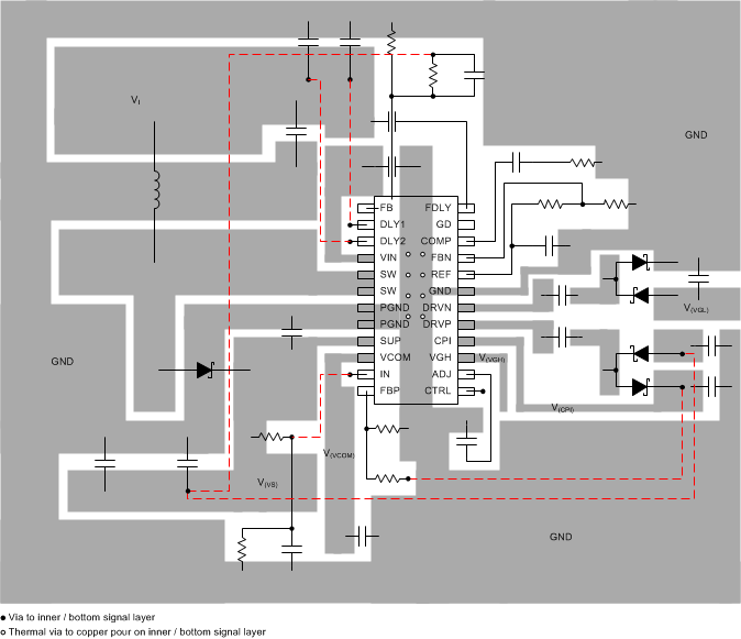
10.2 Layout Example
 Figure 37. PCB Layout Example