ZHCSBL3C June 2013 – May 2017 TPS65150-Q1
PRODUCTION DATA.
- 1 特性
- 2 应用
- 3 说明
- 4 修订历史记录
- 5 Pin Configuration and Functions
- 6 Specifications
- 7 Detailed Description
-
8 Application and Implementation
- 8.1 Application Information
- 8.2
Typical Application
- 8.2.1 Design Requirements
- 8.2.2
Detailed Design Procedure
- 8.2.2.1 Boost Converter Design Procedure
- 8.2.2.2 Rectifier Diode Selection
- 8.2.2.3 Setting the Output Voltage
- 8.2.2.4 Output Capacitor Selection
- 8.2.2.5 Input Capacitor Selection
- 8.2.2.6 Compensation
- 8.2.2.7 Negative Charge Pump
- 8.2.2.8 Positive Charge Pump
- 8.2.2.9 Gate Voltage Shaping
- 8.2.2.10 Power-On Sequencing
- 8.2.2.11 Fault Delay
- 8.2.3 Application Curves
- 8.3 System Examples
- 9 Power Supply Recommendations
- 10Layout
- 11器件和文档支持
- 12机械、封装和可订购信息
8 Application and Implementation
NOTE
Information in the following applications sections is not part of the TI component specification, and TI does not warrant its accuracy or completeness. TI’s customers are responsible for determining suitability of components for their purposes. Customers should validate and test their design implementation to confirm system functionality.
8.1 Application Information
The TPS65150-Q1 device has been designed to provide the input supply voltages for the source drivers and gate drivers plus the voltage for the common plane in LCD display applications. In addition, the device provides a gate voltage shaping function that can be used to modulate the gate drivers' positive supply to reduce image sticking.
8.2 Typical Application
Figure 17 shows a typical application circuit for a monitor display powered from a 5-V supply. It generates up to 450 mA at 13.5 V to power the source drivers, and 20 mA at 23 V and –5 V to power the gate drivers.
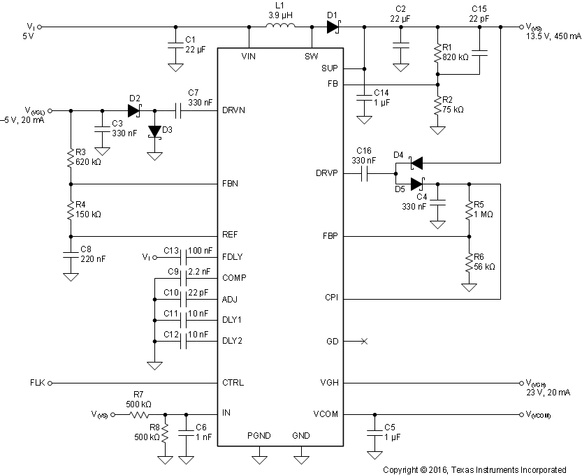 Figure 17. Monitor LCD Supply Powered from a 5-V Rail
8.2.1 Design Requirements
Table 3 shows the parameters for this example.
Table 3. Design Parameters
| PARAMETER | VALUE | |
|---|---|---|
| VI | Input supply voltage | 5 V |
| V(VS) | Boost converter output voltage and current | 13.5 V at 450 mA |
| V(VS)(PP) | Boost converter peak-to-peak output voltage ripple | 10 mV |
| V(CPI) | Positive charge pump output voltage and current | 23 V at 20 mA |
| V(VGH)(PP) | Positive charge pump peak-to-peak output voltage ripple | 100 mV |
| V(VGL) | Negative charge pump output voltage and current | –5 V at 20 mA |
| V(VGL)(PP) | Negative charge pump peak-to-peak output voltage ripple | 100 mV |
| td1 | Negative charge pump start-up delay time | 1 ms |
| td2 | Positive charge pump start-up delay time | 1 ms |
| td(fault) | Fault delay time | 45 ms |
| Gate voltage shaping slope | 10 V/µs | |
8.2.2 Detailed Design Procedure
8.2.2.1 Boost Converter Design Procedure
8.2.2.1.1 Inductor Selection
Several inductors work with the TPS65150-Q1, and with external compensation the performance can be adjusted to the specific application requirements.
The main parameter for the inductor selection is the inductor saturation current, which must be higher than the peak switch current as calculated in Equation 2 with additional margin to cover for heavy load transients. The alternative, more conservative approach, is to choose the inductor with a saturation current at least as high as the maximum switch current limit of 3.4 A.
The second important parameter is the inductor DC resistance. Usually, the lower the DC resistance the higher the efficiency. It is important to note that the inductor DC resistance is not the only parameter determining the efficiency. For a boost converter, where the inductor is the energy storage element, the type and material of the inductor influences the efficiency as well. Especially at a switching frequency of 1.2 MHz, inductor core losses, proximity effects, and skin effects become more important. Usually, an inductor with a larger form factor gives higher efficiency. The efficiency difference between different inductors can vary from 2% to 10%. For the TPS65150-Q1, inductor values from 3.3 µH and 6.8 µH are a good choice, but other values can be used as well. Possible inductors are shown in Table 4. Equivalent parts can also be used.
Table 4. Inductor Selection(1)
| INDUCTANCE | ISAT | DCR | MANUFACTURER | PART NUMBER | DIMENSIONS |
|---|---|---|---|---|---|
| 4.7 µH | 2.6 A | 54 mΩ | Coilcraft | DO1813P-472HC | 8.89 mm × 6.1 mm × 5 mm |
| 4.2 µH | 2.2 A | 23 mΩ | Sumida | CDRH5D28-4R2 | 5.7 mm × 5.7 mm × 3 mm |
| 4.7 µH | 1.6 A | 48 mΩ | Sumida | CDC5D23-4R7 | 6 mm × 6 mm × 2.5 mm |
| 4.2 µH | 1.8 A | 60 mΩ | Sumida | CDRH6D12-4R2 | 6.5 mm × 6.5 mm × 1.5 mm |
| 3.9 µH | 2.6 A | 20 mΩ | Sumida | CDRH6D28-3R9 | 7 mm × 7 mm × 3 mm |
| 3.3 µH | 1.9 A | 50 mΩ | Sumida | CDRH6D12-3R3 | 6.5 mm × 6.5 mm × 1.5 mm |
The first step in the design procedure is to verify whether the maximum possible output current of the boost converter supports the specific application requirements. A simple approach is to estimate the converter efficiency, by taking the efficiency numbers from the provided efficiency curves, or use a worst case assumption for the expected efficiency, for example, 75%.
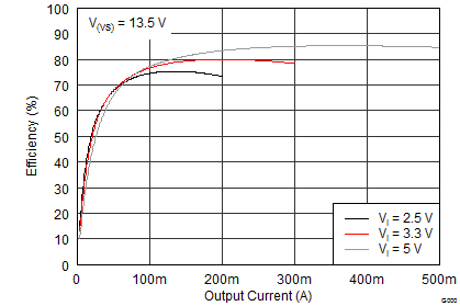
From Figure 19, it can be seen that the boost converter efficiency is about 85% when operating under the target application conditions. Inserting these values into Equation 1 yields Equation 15.

and from Equation 2, the peak switch current can be calculated as Equation 16.

The peak switch current is the peak current that the integrated switch, inductor, and rectifier diode must be able to handle. The calculation must be done for the minimum input voltage where the peak switch current is highest. For the calculation of the maximum current delivered by the boost converter, it must be considered that the positive and negative charge pumps as well as the VCOM buffer run from the output of the boost converter as well.
8.2.2.2 Rectifier Diode Selection
The rectifier diode reverse voltage rating must be higher than the maximum output voltage of the converter (13.5 V in this application); its average forward current rating must be higher than the maximum boost converter output current of 450 mA, and its repetitive peak forward current must be greater than or equal to the peak switch current of 1.8 A. Not all diode manufacturers specify repetitive peak forward current; however, a diode with an average forward current rating of 1 A or higher is suitable for most practical applications.
From Equation 5, the power dissipated in the rectifier diode is calculated with Equation 17.

Table 5 lists a number of suitable rectifier diodes, any of which would be suitable for this application. Equivalent parts can also be used.
Table 5. Rectifier Diode Selection(1)
| IF(AV) | VR | VF | MANUFACTURER | PART NUMBER |
|---|---|---|---|---|
| 2 A | 20 V | 0.44 V at 2 A | Vishay Semiconductor | SL22 |
| 2 A | 20 V | 0.5 V at 2 A | Fairchild Semiconductor | SS22 |
| 1 A | 30 V | 0.44 V at 2 A | Fairchild Semiconductor | MBRS130L |
| 1 A | 20 V | 0.45 V at 1 A | Microsemi | UPS120 |
| 1 A | 20 V | 0.45 V at 1 A | ON Semiconductor | MBRM120 |
8.2.2.3 Setting the Output Voltage
Rearranging Equation 3 and inserting the application parameters yields Equation 18.

Standard values of R1 = 820 kΩ and R2 = 75 kΩ result in a nominal output voltage of 13.68 V and satisfy the recommendation that the value R1 be lower than 1 MΩ.
8.2.2.4 Output Capacitor Selection
For best output voltage filtering, a low ESR output capacitor is recommended. Ceramic capacitors have a low ESR value, but tantalum capacitors can be used as well, depending on the application. A 22-µF ceramic output capacitor works for most applications. Higher capacitor values can be used to improve the load transient regulation. See Table 6 for the selection of the output capacitor.
Rearranging Equation 6 and inserting the application parameters, the minimum value of output capacitance is given by Equation 19.

The closest standard value is 22 µF. In practice, TI recommends connecting an additional 1-µF capacitor directly to the SUP pin to ensure a clean supply to the internal circuitry that runs from this supply voltage.
8.2.2.5 Input Capacitor Selection
For good input voltage filtering, low ESR ceramic capacitors are recommended. A 22-µF ceramic input capacitor is sufficient for most applications. For better input voltage filtering, this value can be increased. See Table 6 for input capacitor recommendations. Equivalent parts can also be used.
Table 6. Input and Output Capacitance Selection
| CAPACITANCE | VOLTAGE RATING | MANUFACTURER | PART NUMBER | SIZE |
|---|---|---|---|---|
| 22 µF | 16 V | Taiyo Yuden | EMK325BY226MM | 1206 |
| 22 µF | 6.3 V | Taiyo Yuden | JMK316BJ226 | 1206 |
8.2.2.6 Compensation
From Table 2, it can be seen that the recommended values for C9 and R9 when VI = 5 V are 2.2 nF and 0 Ω respectively, and that a feedforward zero at 11.2 kHz must be added.
Rearranging Equation 7 yields Equation 20.

Inserting fco = 11.2 kHz and R1 = 820 kΩ yields .

In this case, a standard value of 22 pF was used.
8.2.2.7 Negative Charge Pump
8.2.2.7.1 Choosing the Output Capacitance
Rearranging Equation 9 and inserting the application parameters, the minimum recommended value of C3 is given by Equation 21.

In this application, a capacitor of 330 nF was used to allow the same value to be used for all charge pump capacitors.
8.2.2.7.2 Choosing the Flying Capacitance
A minimum flying capacitance of 100 nF is recommended. In this application, a capacitor of 330 nF was used to allow the same value to be used for all charge pump capacitors.
8.2.2.7.3 Choosing the Feedback Resistors
The ratio of R3 to R4 required to generate an output voltage of –5 V is given by Equation 22.

Values of R3 = 620 kΩ and R4 = 150 kΩ generate a nominal output voltage of –5.014 V and load the REF pin with only 8 µA.
8.2.2.7.4 Choosing the Diodes
The average forward current in D2 and D3 is equal to the output current and therefore a maximum of 20 mA. The peak repetitive forward current in D2 and D3 is equal to twice the output current and therefore less than 40 mA.
The BAT54S comprises two Schottky diodes in a small SOT-23 package and easily meets the current requirements of this application.
8.2.2.8 Positive Charge Pump
8.2.2.8.1 Choosing the Flying Capacitance
A minimum flying capacitor of 330 nF is recommended.
8.2.2.8.2 Choosing the Output Capacitance
Rearranging Equation 10 and inserting the application parameters yields Equation 23.

In this application, a nominal value of 330 nF was used to allow the same value to be used for all charge pump capacitors.
8.2.2.8.3 Choosing the Feedback Resistors
Rearranging Equation 8 and inserting the application parameters yields Equation 24.

Standard values of 1 MΩ and 56 kΩ result in a nominal output voltage of 22.89 V.
8.2.2.8.4 Choosing the Diodes
The average forward current in D4 and D5 is equal to the output current and therefore a maximum of 20 mA. The peak repetitive forward current in D4 and D5 is equal to twice the output current and therefore less than 40 mA.
8.2.2.9 Gate Voltage Shaping
Rearranging Equation 13 and inserting I(ADJ) = 200 µA and slope = 10 V/µs yields Equation 25.

The closest standard value for C10 is 22 pF.
8.2.2.10 Power-On Sequencing
Rearranging Equation 12 and inserting td1 = td2 = 1 ms and Vref2 = 1.213 V, yields Equation 26.

10 nF is the closest standard value.
8.2.2.11 Fault Delay
Rearranging Equation 14 and inserting td(FDLY) = 45 ms yields Equation 27.

100 nF is a standard value.
8.2.3 Application Curves
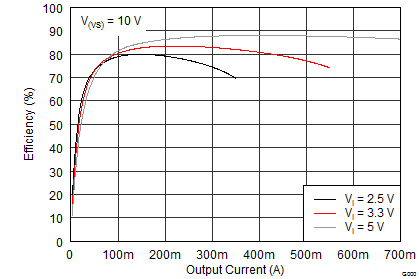
| I(VGH) = 0 mA | I(VGL) = 0 mA |
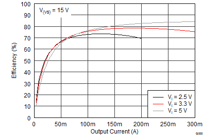
| I(VGH) = 0 mA | I(VGL) = 0 mA |
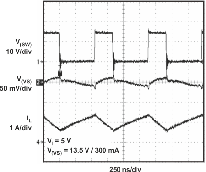
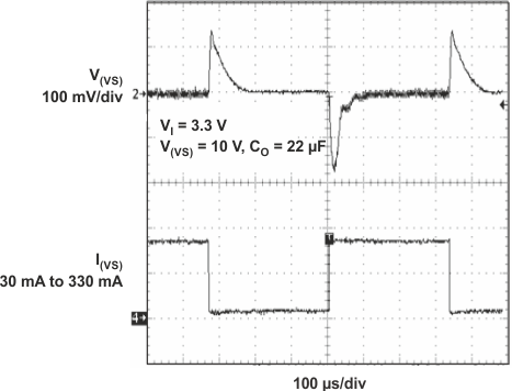 Figure 24. Boost Converter Load Transient Response
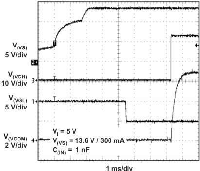 Figure 26. Power-On Sequencing
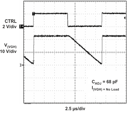 Figure 28. Gate Voltage Shaping
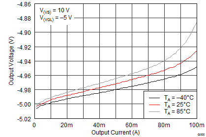
| I(VGH) = 0 mA | I(VGL) = 0 mA |
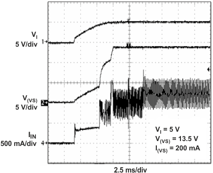 Figure 25. Boost Converter Soft Start
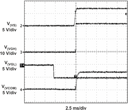 Figure 27. Power-On Sequencing With External Isolation MOSFET
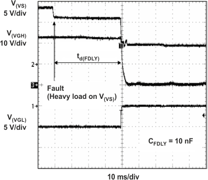 Figure 29. Adjustable Fault Detection Time
8.3 System Examples
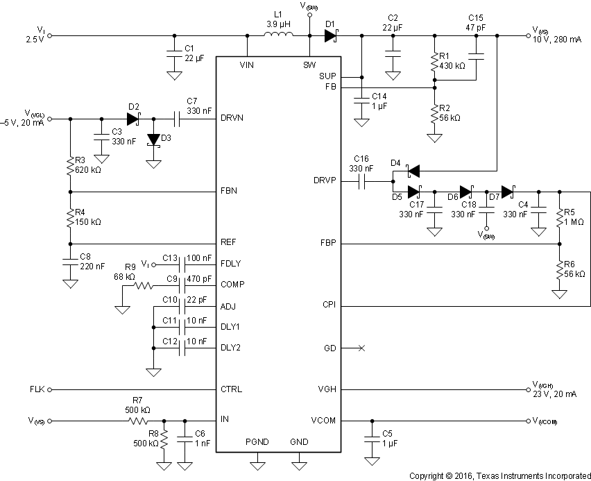 Figure 34. Notebook LCD Supply Powered from a 2.5-V Rail
 Figure 35. Monitor LCD Supply Powered from a 5-V Rail
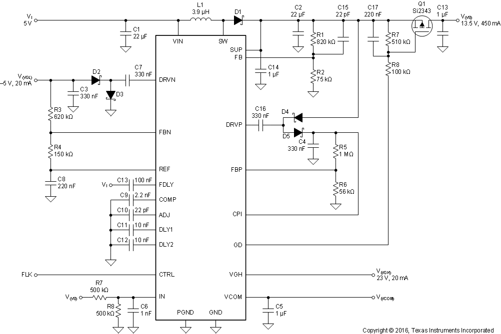 Figure 36. Typical Isolation and Short Circuit Protection Switch for V(VS) Using Q1 and Gate Drive Signal (GD)