ZHCSF63A September 2013 – June 2016 TPS65154
PRODUCTION DATA.
- 1 器件概述
- 2 修订历史记录
- 3 Pin Configuration and Functions
- 4 Specifications
-
5 Detailed Description
- 5.1 Overview
- 5.2 Functional Block Diagram
- 5.3 Feature Description
- 5.4 Device Functional Modes
- 5.5
Programming
- 5.5.1 Configuration
- 5.5.2
Programming Examples (Excluding VCOM)
- 5.5.2.1 Writing to a Single RAM Register
- 5.5.2.2 Writing to Multiple RAM Registers
- 5.5.2.3 Saving Contents of all RAM Registers to EEPROM
- 5.5.2.4 Reading from a Single RAM Register
- 5.5.2.5 Reading from a Single EEPROM Register
- 5.5.2.6 Reading from Multiple RAM Registers
- 5.5.2.7 Reading from Multiple EEPROM Registers
- 5.5.3 Programming Examples - VCOM
- 5.6
Register Map
- 5.6.1
Configuration Registers (Excluding VCOM)
- 5.6.1.1 CONFIG (00h)
- 5.6.1.2 VCC (01h)
- 5.6.1.3 DLY1 (02h)
- 5.6.1.4 AVDD (03h)
- 5.6.1.5 FSW1 (04h)
- 5.6.1.6 SS2 (05h)
- 5.6.1.7 DLY2 (06h)
- 5.6.1.8 VGL (07h)
- 5.6.1.9 SS3 (08h)
- 5.6.1.10 DLY3 (09h)
- 5.6.1.11 VGH (0Ah)
- 5.6.1.12 SS4 (0Bh)
- 5.6.1.13 FSW3 (0Ch)
- 5.6.1.14 DLY4 (0Dh)
- 5.6.1.15 OVP (0Eh)
- 5.6.1.16 FDIM (OFh)
- 5.6.1.17 RESET (10h)
- 5.6.1.18 VDET (11h)
- 5.6.1.19 DLY6 (12h)
- 5.6.1.20 VMAX (13h)
- 5.6.1.21 VMIN (14h)
- 5.6.1.22 USER (15h)
- 5.6.1.23 CONTROL (FFh)
- 5.6.2 VCOM Registers
- 5.6.1
Configuration Registers (Excluding VCOM)
- 6 Application and Implementation
- 7 Power Supply Recommendations
- 8 Layout
- 9 器件和文档支持
- 10机械、封装和可订购信息
8 Layout
8.1 Layout Guidelines
The PCB layout is an important step in a power supply design. An incorrect layout can cause converter instability, load regulation problems, noise, and EMI issues. The list of recommendations below highlights the most important points to consider when doing the layout for the TPS65154 device. However, all PCB layout is a trade-off between theory and practice, and some compromise is always necessary.
- If possible, use a 4-layer PCB. Route high di/dt signals on layer 1 and use the second layer to form a solid ground plane. If a 2-layer PCB is used, route high di/dt signals on layer 1 and add a copper pour connected to ground on the bottom layer.
- Place a decoupling capacitor close to the VIN pin. Use short, wide traces on layer 1 to connect to it.
- Place at least one of the boost converter 1 output capacitors close to the device. Use short, wide traces on layer 1 to connect it between pins 3 and 4, and pin 6.
- Place the boost converter 3 rectifier diode and output capacitor close to the device. Use short, wide traces on layer 1 to connect them to pins 9 and 10.
- Place the boost converter 2 rectifier diode and output capacitor close to the device. Use short, wide traces on layer 1 to connect them to pins 33 and 34.
- Place the flying capacitor connected to pins 19 and 20 and the output capacitor connected to pin 18 close to the device. Use short, wide traces on layer 1 to connect to them.
- Place the VCOM buffer decoupling capacitor connected between pin 2 and pin 47 close to the device. Use short, wide traces on layer 1 to connect to it.
- Route the signals to the compensation components connected to pin 7, pin 40 and pin 46 away from noisy signals.
- Use thermal vias to connect the thermal pad to a large, unbroken copper ground plane (typically, on layer 2).
8.2 Layout Example
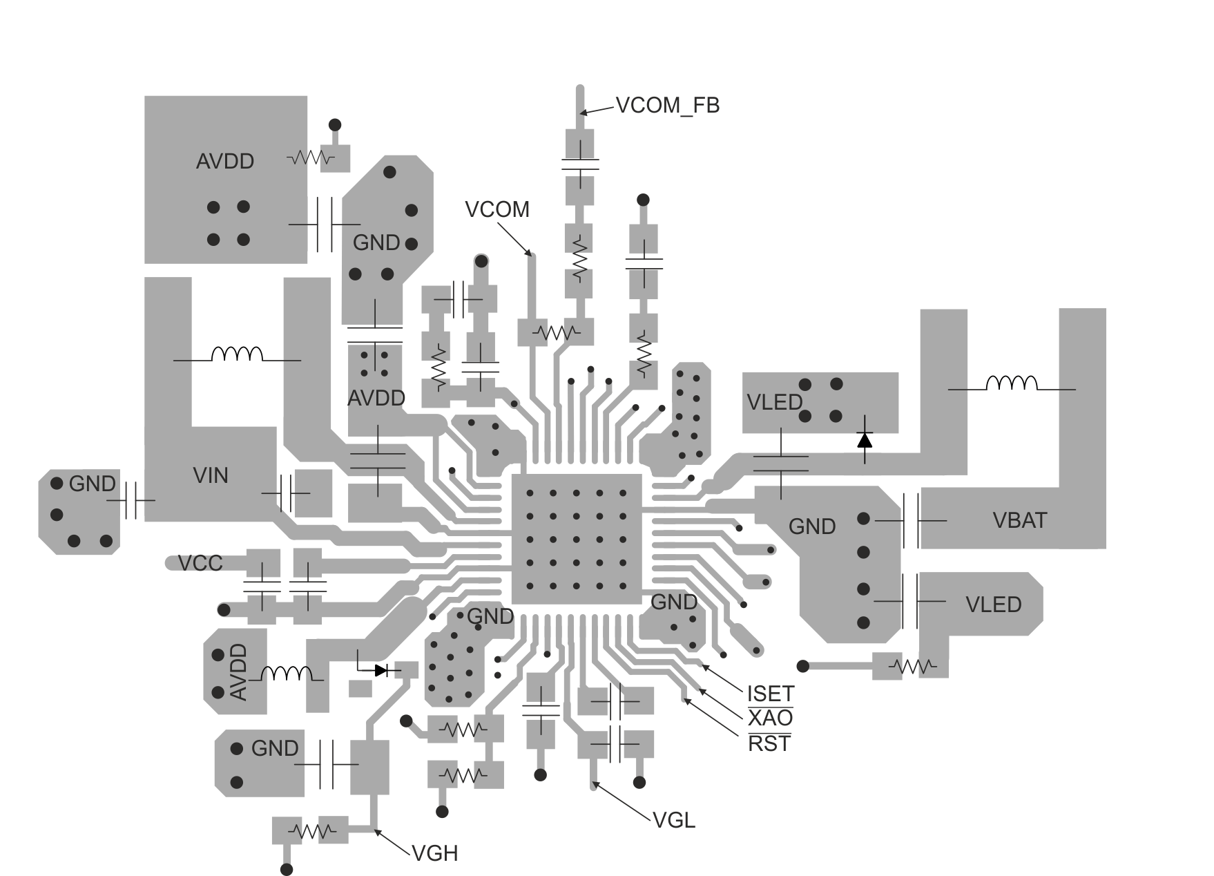
Figure 8-1 shows the main features of the TPS65154 Evaluation Module PCB layout.
 Figure 8-1 Example PCB Layout