ZHCSEO1C March 2012 – February 2016 TPS65177 , TPS65177A
PRODUCTION DATA.
- 1 特性
- 2 应用
- 3 说明
- 4 修订历史记录
- 5 Pin Configuration and Functions
- 6 Specifications
-
7 Detailed Description
- 7.1 Overview
- 7.2 Functional Block Diagram
- 7.3 Feature Description
- 7.4
Device Functional Modes
- 7.4.1 Boost Converter (V(AVDD))
- 7.4.2 Buck 1 Converter (V(IO))
- 7.4.3 BUCK 2 CONVERTER (V(CORE))
- 7.4.4 Buck 3 Converter (V(HAVDD))
- 7.4.5 Positive Charge Pump Controller (V(GH)) with Temperature Compensation
- 7.4.6 Negative Charge Pump Controller (V(GL))
- 7.5 Gate Pulse Modulation (V(GHM))
- 7.6
Programming
- 7.6.1 I2C Serial Interface Description
- 7.6.2 Memory Description
- 7.6.3 Read / Write Description
- 7.6.4 Write Operation
- 7.6.5 READ OPERATION
- 7.6.6 Write Single Data to DAC:
- 7.6.7 Write Multiple Data to DAC (Auto Increment Address):
- 7.6.8 Write all DAC Data to EEPROM:
- 7.6.9 Read Single Data From DAC / EEPROM:
- 7.6.10 Read Multiple Data fFom DAC / EEPROM (Auto Increment Address):
- 7.7
Register Map
- 7.7.1
Registers and DAC Settings
- 7.7.1.1 Channel Register (with factory value) - 00h (00h)
- 7.7.1.2 Boost Output Voltage V(AVDD) Register (with factory value) - 01h (0Fh)
- 7.7.1.3 Boost HVS Offset Voltage Register (with factory value) - 02h (05h)
- 7.7.1.4 Boost Current Limit Negative Offset Current Register (with factory value) - 03h (00h)
- 7.7.1.5 Boost Soft-start Time Register (with factory value) - 04h (00h)
- 7.7.1.6 Buck 1 Output Voltage V(IO) Register (with factory value) - 05h (03h):
- 7.7.1.7 Buck 2 Output Voltage V(CORE) Register (with factory value) - 06h (02h)
- 7.7.1.8 Buck 3 Output Voltage V(HAVDD) Register (with factory value) - 07h (1Bh)
- 7.7.1.9 Pos. Charge Pump Low Output Voltage V(GH_L) Register (with factory value) - 08h (08h):
- 7.7.1.10 Positive Charge Pump Low Output Voltage V(GH_L) to V(GH_H) Positive Offset Voltage V(GH_OFS) Register (with factory value) - 09h (04h):
- 7.7.1.11 Gate Pulse Modulation Limit Voltage Register (with factory value) - 0Ah (00h)
- 7.7.1.12 Negative Charge Pump Output Voltage V(GL) Register (with factory value) - 0Bh (04h)
- 7.7.1.13 Buck 3 HVS Offset Voltage Register (with factory value) - 0Ch (00h):
- 7.7.1.14 Memory Write Remain Time Register (with factory value) - FEh (0Fh):
- 7.7.1
Registers and DAC Settings
- 8 Application and Implementation
- 9 Power Supply Recommendations
- 10Layout
- 11器件和文档支持
- 12机械、封装和可订购信息
10 Layout
10.1 Layout Guideline
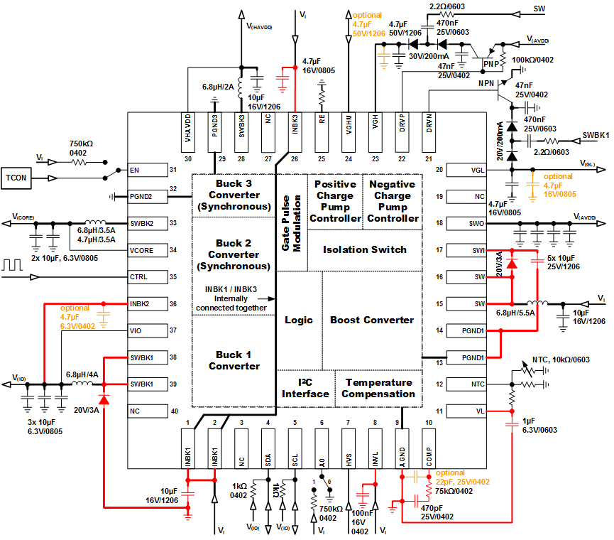
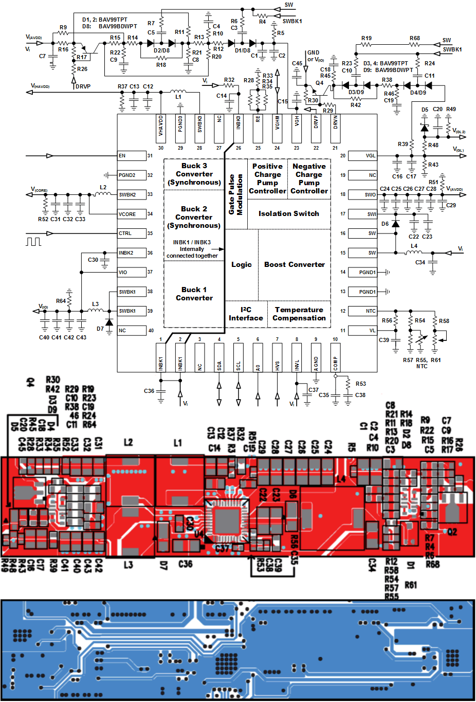
The PCB layout is a very important step in the power supply design. Following points should be considered.
- Place red marked components first and as close as possible to the device, keep red lines short.
- The bolder the line the wider the trace should be on the PCB because bold lines carry high currents.
- The input capacitors for INBK1, INBK3 and INVL should be placed as close as possible to the IC.
- For V(AVDD) the line SW, Diode, SWI as well as the connection PGND to SWI capacitor should be kept short and low resistive.
- The compensation network for the Boost converter V(AVDD) must be placed as close as possible to the IC and connected by short lines to COMP and AGND to avoid noise coupling.
- For V(IO) the line SWBK1, Diode, GND of INBK1 capacitor should be kept short and low resistive.
- For V(CORE) an additional input capacitor should be used when the V(IO) output capacitor line is longer than 1 cm or a wide connection line is not possible to stabilize the input voltage.
- Feedback lines starting at the output capacitors should be routed through a non noisy area away from switching traces. If possible the feedback lines should be kept short to reduce noise coupling.
- Inductors can be placed further away from the IC to avoid IC heating through the inductor.
- All IC Grounds (AGND, PGNDx) must be connected to the Exposed Thermal PAD.
- Avoid vias in Power lines when possible because of their high inductance and resistance.
- The Exposed Thermal PAD of the QFN package must be soldered to a big GND cooling area. For good thermal conduction to the cooling area as much as possible vias should be used to keep the device cool.
- The thermal resistor NTC should be placed away from heat sources. For most accurate environment temperature measurement the NTC must be placed at the coldest point of the PCB.

