ZHCSJX9 June 2019 TPS652170
PRODUCTION DATA.
- 1 特性
- 2 应用
- 3 说明
- 4 修订历史记录
- 5 Pin Configuration and Functions
- 6 Specifications
-
7 Detailed Description
- 7.1 Overview
- 7.2 Functional Block Diagram
- 7.3
Feature Description
- 7.3.1 Wake-Up and Power-Up Sequencing
- 7.3.2 Power Good
- 7.3.3 Push-Button Monitor (PB_IN)
- 7.3.4 nWAKEUP Pin (nWAKEUP)
- 7.3.5 Power Enable Pin (PWR_EN)
- 7.3.6 Reset Pin (nRESET)
- 7.3.7 Interrupt Pin (nINT)
- 7.3.8 Analog Multiplexer
- 7.3.9 Battery Charger and Power Path
- 7.3.10 Battery Charging
- 7.3.11 Precharge
- 7.3.12 Charge Termination
- 7.3.13 Battery Detection and Recharge
- 7.3.14 Safety Timer
- 7.3.15 Battery-Pack Temperature Monitoring
- 7.3.16 DC/DC Converters
- 7.3.17 Standby LDO Regulators (LDO1, LDO2)
- 7.3.18 Load Switches or LDO Regulators (LS1 or LDO3, LS2 or LDO4)
- 7.3.19 White LED Driver
- 7.4 Device Functional Modes
- 7.5 Programming
- 7.6
Register Maps
- 7.6.1 Register Address Map
- 7.6.2 Chip ID Register (CHIPID) (Address = 0x00) [reset = 0x02]
- 7.6.3 Power Path Control Register (PPATH) (Address = 0x01) [reset = 0x3D]
- 7.6.4 Interrupt Register (INT) (Address = 0x02) [reset = 0x80]
- 7.6.5 Charger Configuration Register 0 (CHGCONFIG0) (Address = 0x03) [reset = 0x00]
- 7.6.6 Charger Configuration Register 1 (CHGCONFIG1) (Address = 0x04) [reset = 0xB1]
- 7.6.7 Charger Configuration Register 2 (CHGCONFIG2) (Address = 0x05) [reset = 0x80]
- 7.6.8 Charger Configuration Register 3 (CHGCONFIG3) (Address = 0x06) [reset = 0xB2]
- 7.6.9 WLED Control Register 1 (WLEDCTRL1) (Address = 0x07) [reset = 0xB1]
- 7.6.10 WLED Control Register 2 (WLEDCTRL2) (Address = 0x08) [reset = 0x00]
- 7.6.11 MUX Control Register (MUXCTRL) (Address = 0x09) [reset = 0x00]
- 7.6.12 Status Register (STATUS) (Address = 0x0A) [reset = 0x00]
- 7.6.13 Password Register (PASSWORD) (Address = 0x0B) [reset = 0x00]
- 7.6.14 Power Good Register (PGOOD) (Address = 0x0C) [reset = 0x00]
- 7.6.15 Power-Good Control Register (DEFPG) (Address = 0x0D) [reset = 0x0C]
- 7.6.16 DCDC1 Control Register (DEFDCDC1) (Address = 0x0E) [reset = 0x18]
- 7.6.17 DCDC2 Control Register (DEFDCDC2) (Address = 0x0F) [reset = 0x08]
- 7.6.18 DCDC3 Control Register (DEFDCDC3) (Address = 0x10) [reset = 0x08]
- 7.6.19 Slew-Rate Control Register (DEFSLEW) (Address = 0x11) [reset = 0x06]
- 7.6.20 LDO1 Control Register (DEFLDO1) (Address = 0x12) [reset = 0x09]
- 7.6.21 LDO2 Control Register (DEFLDO2) (Address = 0x13) [reset = 0x38]
- 7.6.22 Load Switch1 or LDO3 Control Register (DEFLS1) (Address = 0x14) [reset = 0x26]
- 7.6.23 Load Switch2 or LDO4 Control Register (DEFLS2) (Address = 0x15) [reset = 0x3F]
- 7.6.24 Enable Register (ENABLE) (Address = 0x16) [reset = 0x00]
- 7.6.25 UVLO Control Register (DEFUVLO) (Address = 0x18) [reset = 0x00]
- 7.6.26 Sequencer Register 1 (SEQ1) (Address = 0x19) [reset = 0x00]
- 7.6.27 Sequencer Register 2 (SEQ2) (Address = 0x1A) [reset = 0x00]
- 7.6.28 Sequencer Register 3 (SEQ3) (Address = 0x1B) [reset = 0x00]
- 7.6.29 Sequencer Register 4 (SEQ4) (Address = 0x1C) [reset = 0x40]
- 7.6.30 Sequencer Register 5 (SEQ5) (Address = 0x1D) [reset = 0x20]
- 7.6.31 Sequencer Register 6 (SEQ6) (Address = 0x1E) [reset = 0x00]
- 8 Application and Implementation
- 9 Power Supply Recommendations
- 10Layout
- 11器件和文档支持
- 12机械、封装和可订购信息
封装选项
请参考 PDF 数据表获取器件具体的封装图。
机械数据 (封装 | 引脚)
- RSL|48
散热焊盘机械数据 (封装 | 引脚)
- RSL|48
订购信息
7.3.1.1 Power-Up Sequencing
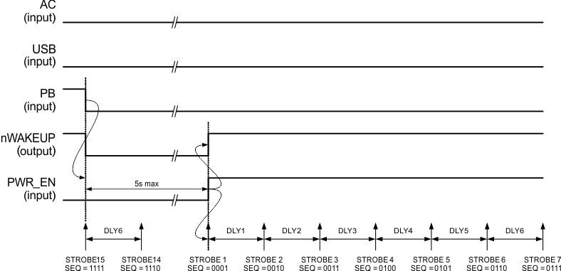
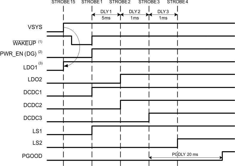
When the power-up sequence is initiated, STROBE1 occurs and any rail assigned to this strobe is enabled. After a delay time of DLY1, STROBE2 occurs and the rail assigned to this strobe is powered up. The sequence continues until all strobes have occurred and all DLYx times have been executed.

The default power-up sequence can be changed by writing to the SEQ1 through SEQ6 registers. Strobes are assigned to rails by writing to the SEQ1 through SEQ4 registers. A rail can be assigned to only one strobe but multiple rails can be assigned to the same strobe. Delays between strobes are defined in the SEQ5 and SEQ6 registers.

The power-up sequence is executed if the following events occurs:
From the OFF state (going to the ACTIVE state):
- Push-button is pressed (falling edge on PB_IN) OR
- USB voltage is asserted (rising edge on USB) OR
- The AC adaptor is inserted (rising edge on the AC pin)
The PWR_EN pin is level-sensitive (opposed to edge-sensitive), and the pin can be asserted before or after the previously listed power-up events. However, the PWR_EN pin must be asserted within 5 s of the power-up event; otherwise, the power-down sequence is triggered and the device goes to the OFF state. If a fault occurs because the device is in undervoltage lockout (UVLO) or requires overtemperature shutdown (OTS), the device goes to the OFF state.
From the SLEEP state (going to the ACTIVE state):
- The push-button is pressed (falling edge on the PB_IN pin) OR
- The USB voltage is asserted (rising edge on the USB pin) OR
- The AC adaptor is inserted (rising edge on the AC pin) OR
- The PWR_EN pin is asserted (pulled high).
In the SLEEP state, the power-up sequence can be triggered by asserting the PWR_EN pin only, and the push-button press or AC and USB assertion are not required. If a fault occurs because the device is in undervoltage lockout (UVLO) or requires overtemperature shutdown (OTS), the device goes to the OFF state.
In the ACTIVE state:
The sequencer can be triggered any time by setting the SEQUP bit in the SEQ6 register high. The SEQUP bit is automatically cleared after the sequencer is complete.
Rails that are not assigned to a strobe (the SEQ bit set to 0000b) are not affected by power-up and power-down sequencing and stay in their current ON or OFF state regardless of the sequencer. Any rail can be enabled or disabled at any time by setting the corresponding enable bit in the ENABLE register with the only exception that the ENABLE register cannot be accessed while the sequencer is active. Enable bits always reflect the current enable state of the rail, that is, the sequencer sets or resets the enable bits for the rails under its control. Also, whenever faults occur which shut-down the power-rails, the corresponding enable bits are reset.