ZHCSJX9 June   2019 TPS652170

PRODUCTION DATA.  

  1. 特性
  2. 应用
  3. 说明
    1.     Device Images
      1.      简化应用示意图
  4. 修订历史记录
  5. Pin Configuration and Functions
    1.     Pin Functions
  6. Specifications
    1. 6.1 Absolute Maximum Ratings
    2. 6.2 ESD Ratings
    3. 6.3 Recommended Operating Conditions
    4. 6.4 Thermal Information
    5. 6.5 Electrical Characteristics
    6. 6.6 I2C Timing Requirements
    7. 6.7 Typical Characteristics
  7. Detailed Description
    1. 7.1 Overview
    2. 7.2 Functional Block Diagram
    3. 7.3 Feature Description
      1. 7.3.1  Wake-Up and Power-Up Sequencing
        1. 7.3.1.1 Power-Up Sequencing
        2. 7.3.1.2 Power-Down Sequencing
        3. 7.3.1.3 Special Strobes (STROBE 14 and 15)
      2. 7.3.2  Power Good
        1. 7.3.2.1 LDO1, LDO2 Power-Good (LDO_PGOOD)
        2. 7.3.2.2 Primary Power-Good (PGOOD)
        3. 7.3.2.3 Load Switch PGOOD
      3. 7.3.3  Push-Button Monitor (PB_IN)
      4. 7.3.4  nWAKEUP Pin (nWAKEUP)
      5. 7.3.5  Power Enable Pin (PWR_EN)
      6. 7.3.6  Reset Pin (nRESET)
      7. 7.3.7  Interrupt Pin (nINT)
      8. 7.3.8  Analog Multiplexer
      9. 7.3.9  Battery Charger and Power Path
        1. 7.3.9.1 Shorted or Absent Battery (VBAT < 1.5 V)
        2. 7.3.9.2 Dead Battery (1.5 V < VBAT < VUVLO)
        3. 7.3.9.3 Good Battery (VBAT > VUVLO)
        4. 7.3.9.4 AC and USB Input Discharge
      10. 7.3.10 Battery Charging
      11. 7.3.11 Precharge
      12. 7.3.12 Charge Termination
      13. 7.3.13 Battery Detection and Recharge
      14. 7.3.14 Safety Timer
        1. 7.3.14.1 Dynamic Timer Function
        2. 7.3.14.2 Timer Fault
      15. 7.3.15 Battery-Pack Temperature Monitoring
      16. 7.3.16 DC/DC Converters
        1. 7.3.16.1 Operation
        2. 7.3.16.2 Output Voltage Setting
        3. 7.3.16.3 Power-Save Mode and Pulse-Frequency Modulation (PFM)
        4. 7.3.16.4 Dynamic Voltage Positioning
        5. 7.3.16.5 100% Duty-Cycle Low-Dropout Operation
        6. 7.3.16.6 Short-Circuit Protection
        7. 7.3.16.7 Soft Start
      17. 7.3.17 Standby LDO Regulators (LDO1, LDO2)
      18. 7.3.18 Load Switches or LDO Regulators (LS1 or LDO3, LS2 or LDO4)
      19. 7.3.19 White LED Driver
    4. 7.4 Device Functional Modes
      1. 7.4.1 PMIC States
        1. 7.4.1.1 OFF State
        2. 7.4.1.2 ACTIVE State
        3. 7.4.1.3 SLEEP State
        4. 7.4.1.4 RESET State
    5. 7.5 Programming
      1. 7.5.1 I2C Bus Operation
      2. 7.5.2 Password Protection
        1. 7.5.2.1 Level1 Protection
        2. 7.5.2.2 Level2 Protection
      3. 7.5.3 Resetting of Registers to Default Values
    6. 7.6 Register Maps
      1. 7.6.1  Register Address Map
        1. 7.6.1.1 Programming Power-Up Default Values
      2. 7.6.2  Chip ID Register (CHIPID) (Address = 0x00) [reset = 0x02]
        1. Table 2. CHIPID Register Field Descriptions
      3. 7.6.3  Power Path Control Register (PPATH) (Address = 0x01) [reset = 0x3D]
        1. Table 3. PPATH Register Field Descriptions
      4. 7.6.4  Interrupt Register (INT) (Address = 0x02) [reset = 0x80]
        1. Table 4. INT Register Field Descriptions
      5. 7.6.5  Charger Configuration Register 0 (CHGCONFIG0) (Address = 0x03) [reset = 0x00]
        1. Table 5. CHGCONFIG0 Register Field Descriptions
      6. 7.6.6  Charger Configuration Register 1 (CHGCONFIG1) (Address = 0x04) [reset = 0xB1]
        1. Table 6. CHGCONFIG1 Register Field Descriptions
      7. 7.6.7  Charger Configuration Register 2 (CHGCONFIG2) (Address = 0x05) [reset = 0x80]
        1. Table 7. CHGCONFIG2 Register Field Descriptions
      8. 7.6.8  Charger Configuration Register 3 (CHGCONFIG3) (Address = 0x06) [reset = 0xB2]
        1. Table 8. CHGCONFIG3 Register Field Descriptions
      9. 7.6.9  WLED Control Register 1 (WLEDCTRL1) (Address = 0x07) [reset = 0xB1]
        1. Table 9. WLEDCTRL1 Register Field Descriptions
      10. 7.6.10 WLED Control Register 2 (WLEDCTRL2) (Address = 0x08) [reset = 0x00]
        1. Table 10. WLEDCTRL2 Register Field Descriptions
      11. 7.6.11 MUX Control Register (MUXCTRL) (Address = 0x09) [reset = 0x00]
        1. Table 11. MUXCTRL Register Field Descriptions
      12. 7.6.12 Status Register (STATUS) (Address = 0x0A) [reset = 0x00]
        1. Table 12. STATUS Register Field Descriptions
      13. 7.6.13 Password Register (PASSWORD) (Address = 0x0B) [reset = 0x00]
        1. Table 13. Password Register (PASSWORD) Field Descriptions
      14. 7.6.14 Power Good Register (PGOOD) (Address = 0x0C) [reset = 0x00]
        1. Table 14. PGOOD Register Field Descriptions
      15. 7.6.15 Power-Good Control Register (DEFPG) (Address = 0x0D) [reset = 0x0C]
        1. Table 15. DEFPG Register Field Descriptions
      16. 7.6.16 DCDC1 Control Register (DEFDCDC1) (Address = 0x0E) [reset = 0x18]
        1. Table 16. DEFDCDC1 Register Field Descriptions
      17. 7.6.17 DCDC2 Control Register (DEFDCDC2) (Address = 0x0F) [reset = 0x08]
        1. Table 17. DEFDCDC2 Register Field Descriptions
      18. 7.6.18 DCDC3 Control Register (DEFDCDC3) (Address = 0x10) [reset = 0x08]
        1. Table 18. DEFDCDC3 Register Field Descriptions
      19. 7.6.19 Slew-Rate Control Register (DEFSLEW) (Address = 0x11) [reset = 0x06]
        1. Table 19. DEFSLEW Register Field Descriptions
      20. 7.6.20 LDO1 Control Register (DEFLDO1) (Address = 0x12) [reset = 0x09]
        1. Table 20. DEFLDO1 Register Field Descriptions
      21. 7.6.21 LDO2 Control Register (DEFLDO2) (Address = 0x13) [reset = 0x38]
        1. Table 21. DEFLDO2 Register Field Descriptions
      22. 7.6.22 Load Switch1 or LDO3 Control Register (DEFLS1) (Address = 0x14) [reset = 0x26]
        1. Table 22. DEFLS1 Register Field Descriptions
      23. 7.6.23 Load Switch2 or LDO4 Control Register (DEFLS2) (Address = 0x15) [reset = 0x3F]
        1. Table 23. DEFLS2 Register Field Descriptions
      24. 7.6.24 Enable Register (ENABLE) (Address = 0x16) [reset = 0x00]
        1. Table 24. ENABLE Register Field Descriptions
      25. 7.6.25 UVLO Control Register (DEFUVLO) (Address = 0x18) [reset = 0x00]
        1. Table 25. DEFUVLO Register Field Descriptions
      26. 7.6.26 Sequencer Register 1 (SEQ1) (Address = 0x19) [reset = 0x00]
        1. Table 26. SEQ1 Register Field Descriptions
      27. 7.6.27 Sequencer Register 2 (SEQ2) (Address = 0x1A) [reset = 0x00]
        1. Table 27. SEQ2 Register Field Descriptions
      28. 7.6.28 Sequencer Register 3 (SEQ3) (Address = 0x1B) [reset = 0x00]
        1. Table 28. SEQ3 Register Field Descriptions
      29. 7.6.29 Sequencer Register 4 (SEQ4) (Address = 0x1C) [reset = 0x40]
        1. Table 29. SEQ4 Register Field Descriptions
      30. 7.6.30 Sequencer Register 5 (SEQ5) (Address = 0x1D) [reset = 0x20]
        1. Table 30. SEQ5 Register Field Descriptions
      31. 7.6.31 Sequencer Register 6 (SEQ6) (Address = 0x1E) [reset = 0x00]
        1. Table 31. SEQ6 Register Field Descriptions
  8. Application and Implementation
    1. 8.1 Application Information
    2. 8.2 Typical Application
      1. 8.2.1 Design Requirements
      2. 8.2.2 Detailed Design Procedure
        1. 8.2.2.1 Output Filter Design (Inductor and Output Capacitor)
          1. 8.2.2.1.1 Inductor Selection for Buck Converters
          2. 8.2.2.1.2 Output Capacitor Selection
          3. 8.2.2.1.3 Input Capacitor Selection
        2. 8.2.2.2 5-V Operation Without a Battery
      3. 8.2.3 Application Curves
  9. Power Supply Recommendations
  10. 10Layout
    1. 10.1 Layout Guidelines
    2. 10.2 Layout Example
  11. 11器件和文档支持
    1. 11.1 器件支持
      1. 11.1.1 第三方米6体育平台手机版_好二三四免责声明
    2. 11.2 文档支持
      1. 11.2.1 相关文档
    3. 11.3 接收文档更新通知
    4. 11.4 社区资源
    5. 11.5 商标
    6. 11.6 静电放电警告
    7. 11.7 Glossary
  12. 12机械、封装和可订购信息

封装选项

请参考 PDF 数据表获取器件具体的封装图。

机械数据 (封装 | 引脚)
  • RSL|48
散热焊盘机械数据 (封装 | 引脚)
订购信息

Timer Fault

A timer fault occurs if the battery voltage does not exceed the VLOWV voltage in the tPRECHG time during precharging. A timer fault also occurs if the battery current does not reach the ITERM current in fast charge before the safety timer expires. Fast-charge time is measured from the start of the fast-charge cycle.

The fault status is indicated by the CHTOUT and PCHTOUT bits in the CHGCONFIG0 register. Time-out faults are cleared and a new charge cycle is started when either the USB or AC supply is connected (rising edge of VUSB or VAC), the charger RESET bit is set to 1b in the CHGCONFIG1 register, or the battery voltage decreases to less than the recharge threshold (VRCH).
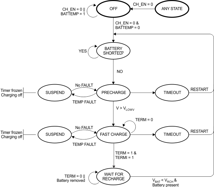
TPS652170 battery_charger_state_diagram_lvsb64.gif
TEMP FAULT = Battery HOT || Battery cold || Thermal shutdown
RESTART = VUSB (↑) || VAC (↑) || Charger RESET bit (↑) || VBAT < VRCH
Figure 15. State Diagram of Battery Charger