ZHCSD17E November 2014 – February 2021 TPS65218
PRODUCTION DATA
- 1 特性
- 2 应用
- 3 说明
- 4 Revision History
- 5 Pin Configuration and Functions
- 6 Specifications
-
7 Detailed Description
- 7.1 Overview
- 7.2 Functional Block Diagram
- 7.3
Feature Description
- 7.3.1
Wake-Up and Power-Up and Power-Down Sequencing
- 7.3.1.1 Power-Up Sequencing
- 7.3.1.2 Power-Down Sequencing
- 7.3.1.3 Strobe 1 and Strobe 2
- 7.3.1.4 Supply Voltage Supervisor and Power-Good (PGOOD)
- 7.3.1.5 Backup Supply Power-Good (PGOOD_BU)
- 7.3.1.6 Internal LDO (INT_LDO)
- 7.3.1.7 Current Limited Load Switches
- 7.3.1.8 LDO1
- 7.3.1.9 Coin Cell Battery Voltage Acquisition
- 7.3.1.10 UVLO
- 7.3.1.11 Power-Fail Comparator
- 7.3.1.12 Battery-Backup Supply Power-Path
- 7.3.1.13 DCDC3 and DCDC4 Power-Up Default Selection
- 7.3.1.14 I/O Configuration
- 7.3.1.15 Push Button Input (PB)
- 7.3.1.16 AC_DET Input (AC_DET)
- 7.3.1.17 Interrupt Pin (INT)
- 7.3.1.18 I2C Bus Operation
- 7.3.1
Wake-Up and Power-Up and Power-Down Sequencing
- 7.4 Device Functional Modes
- 7.5 Register Maps
- 8 Application and Implementation
- 9 Power Supply Recommendations
- 10Layout
- 11Device and Documentation Support
- 12Mechanical, Packaging, and Orderable Information
封装选项
机械数据 (封装 | 引脚)
散热焊盘机械数据 (封装 | 引脚)
订购信息
7.3.1.10 UVLO
Depending on the slew rate of the input voltage into the IN_BIAS pin, the power rails of TPS65218 will be enabled at either VULVO or VULVO + VHYS.
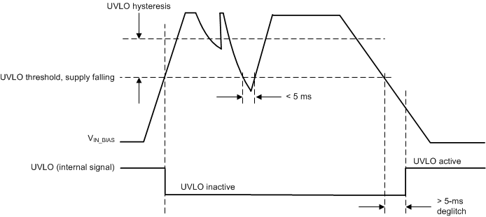
If the slew rate of the IN_BIAS voltage is greater than 30 V/s, then TPS65218 will power up at VULVO. Once the input voltage rises above this level, the input voltage may drop to the VUVLO level before the PMIC shuts down. In this scenario, if the input voltage were to fall below VUVLO but above 2.55 V, the input voltage would have to recover above VUVLO in less than 5 ms for the device to remain active.
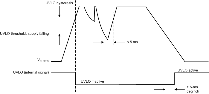
If the slew rate of the IN_BIAS voltage is less than 30 V/s, then TPS65218 will power up at VULVO + VHYS. Once the input voltage rises above this level, the input voltage may drop to the VUVLO level before the PMIC shuts down. In this scenario, if the input voltage were to fall below VUVLO but above 2.5 V, the input voltage would have to recover above VUVLO + VHYS in less than 5 ms for the device to remain active.
In either slew rate scenario, if the input voltage were to fall below 2.5 V, the digital core is reset and all remaining power rails are shut down instantaneously and are pulled low to ground by their internal discharge circuitry (DCDC1-4 and LDO1).
 Figure 7-14 Definition of UVLO and Hysteresis, IN_BIAS Slew Rate > 30 V/s
 Figure 7-15 Definition of UVLO and
Hysteresis,
IN_BIAS Slew Rate < 30 V/s
Figure 7-15 Definition of UVLO and
Hysteresis,
IN_BIAS Slew Rate < 30 V/sAfter the UVLO triggers, the internal LDO blocks current flow from its output capacitor back to the IN_BIAS pin, allowing the digital core and the discharge circuits to remain powered for a limited amount of time to properly shut-down and discharge the output rails. The hold-up time is determined by the value of the capacitor connected to INT_LDO. See Section 7.3.1.6 for more details.