ZHCSKD3A November 2019 – February 2021 TPS6521815
PRODUCTION DATA
- 1 特性
- 2 应用
- 3 说明
- 4 Revision History
- 5 Description (continued)
- 6 Pin Configuration and Functions
- 7 Specifications
-
8 Detailed Description
- 8.1 Overview
- 8.2 Functional Block Diagram
- 8.3
Feature Description
- 8.3.1
Wake-Up and Power-Up and Power-Down Sequencing
- 8.3.1.1 Power-Up Sequencing
- 8.3.1.2 Power-Down Sequencing
- 8.3.1.3 Strobe 1 and Strobe 2
- 8.3.1.4 Supply Voltage Supervisor and Power-Good (PGOOD)
- 8.3.1.5 Backup Supply Power-Good (PGOOD_BU)
- 8.3.1.6 Internal LDO (INT_LDO)
- 8.3.1.7 Current Limited Load Switches
- 8.3.1.8 LDO1
- 8.3.1.9 Coin Cell Battery Voltage Acquisition
- 8.3.1.10 UVLO
- 8.3.1.11 Power-Fail Comparator
- 8.3.1.12 Battery-Backup Supply Power-Path
- 8.3.1.13 DCDC3 and DCDC4 Power-Up Default Selection
- 8.3.1.14 I/O Configuration
- 8.3.1.15 Push Button Input (PB)
- 8.3.1.16 AC_DET Input (AC_DET)
- 8.3.1.17 Interrupt Pin (INT)
- 8.3.1.18 I2C Bus Operation
- 8.3.1
Wake-Up and Power-Up and Power-Down Sequencing
- 8.4 Device Functional Modes
- 8.5 Programming
- 8.6 Register Maps
- 9 Application and Implementation
- 10Power Supply Recommendations
- 11Layout
- 12Device and Documentation Support
- 13Mechanical, Packaging, and Orderable Information
8.3.1.15 Push Button Input (PB)
The PB pin is a CMOS-type input used to power-up the PMIC. Typically, the PB pin is connected to a momentary switch to ground and an external pullup resistor. The power-up sequence is triggered if the PB input is held low for 600 ms.
 Figure 8-25 Left: Typical PB Input Circuit Right: Push-Button
Input (PB) Deglitch and Power-Up Timing
Figure 8-25 Left: Typical PB Input Circuit Right: Push-Button
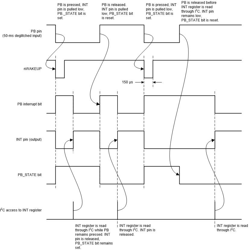
Input (PB) Deglitch and Power-Up TimingIn ACTIVE mode, the TPS6521815 monitors the PB input and issues an interrupt when the pin status changes, such as when it drops below or rises above the PB input-low or input-high thresholds. The interrupt is masked by the PBM bit in the INT_MASK1 register.
 Figure 8-26 PB
Input-Low or Input-High Thresholds
Figure 8-26 PB
Input-Low or Input-High ThresholdsInterrupts are issued whenever the PB pin status changes. The PB_STATE bit reflects the current status of the PB input. nWAKEUP is pulled low for 150 µs on every falling edge of PB.