ZHCSM96A November 2020 – August 2021 TPS6521835
PRODUCTION DATA
- 1 特性
- 2 应用
- 3 说明
- 4 Revision History
- 5 Pin Configuration and Functions
- 6 Specifications
-
7 Detailed Description
- 7.1 Overview
- 7.2 Functional Block Diagram
- 7.3
Feature Description
- 7.3.1
Wake-Up and Power-Up and Power-Down Sequencing
- 7.3.1.1 Power-Up Sequencing
- 7.3.1.2 Power-Down Sequencing
- 7.3.1.3 Strobe 1 and Strobe 2
- 7.3.1.4 Supply Voltage Supervisor and Power-Good (PGOOD)
- 7.3.1.5 Backup Supply Power-Good (PGOOD_BU)
- 7.3.1.6 Internal LDO (INT_LDO)
- 7.3.1.7 Current Limited Load Switches
- 7.3.1.8 LDO1
- 7.3.1.9 Coin Cell Battery Voltage Acquisition
- 7.3.1.10 UVLO
- 7.3.1.11 Power-Fail Comparator
- 7.3.1.12 Battery-Backup Supply Power-Path
- 7.3.1.13 DCDC3 and DCDC4 Power-Up Default Selection
- 7.3.1.14 I/O Configuration
- 7.3.1.15 Push Button Input (PB)
- 7.3.1.16 AC_DET Input (AC_DET)
- 7.3.1.17 Interrupt Pin (INT)
- 7.3.1.18 I2C Bus Operation
- 7.3.1
Wake-Up and Power-Up and Power-Down Sequencing
- 7.4 Device Functional Modes
- 7.5 Register Maps
- 8 Application and Implementation
- 9 Power Supply Recommendations
- 10Layout
- 11Device and Documentation Support
- 12Mechanical, Packaging, and Orderable Information
7.3.1.16 AC_DET Input (AC_DET)
The AC_DET pin is a CMOS-type input used in three different ways to control the power-up of the PMIC:
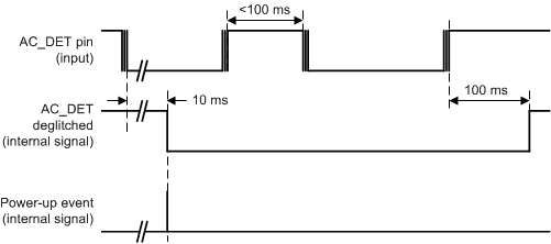
- In a battery operated system, AC_DET is typically connected to an external battery charger with an open-drain power-good output pulled low when a valid charger supply is connected to the system. A falling edge on the AC_DET pin causes the PMIC to power up.
- In a non-portable system, the AC_DET pin may be shorted to ground and the device powers up whenever system power is applied to the chip.
- If none of the above behaviors are desired, AC_DET may be tied to system power (IN_BIAS). Power-up is then controlled through the push-button input or PWR_EN input.

A. Portable Systems
B. Non-portable Systems
C. Disabled
Figure 7-28 AC_DET Pin Configurations Figure 7-29 AC_DET Input Deglitch and Power-Up Timing (Portable Systems)
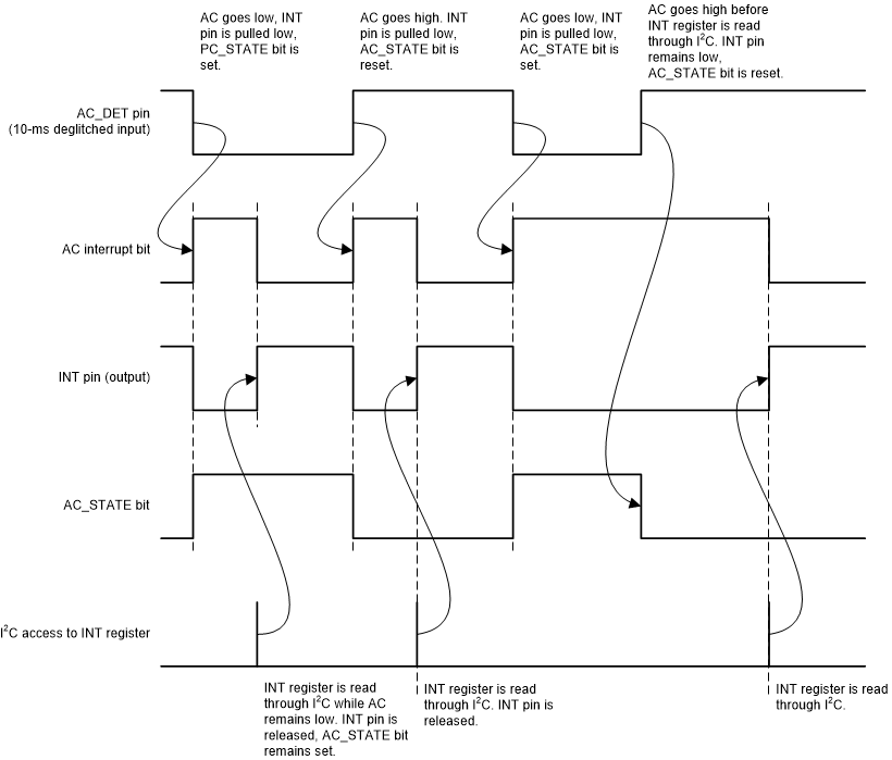
In ACTIVE state, the TPS6521835 monitors the AC_DET input and issues an interrupt when the pin status changes, such as when it drops below or rises above the AC_DET input-low or input-high thresholds. The interrupt is masked by the ACM bit in the INT_MASK1 register.
 Figure 7-30 AC_STATE Pin
Note:
Interrupts are issued whenever the AC_DET pin status changes. The AC_STATE bit reflects the current status of the AC_DET input.