ZHCSH55B December 2017 – September 2018 TPS65218D0
UNLESS OTHERWISE NOTED, this document contains PRODUCTION DATA.
- 1 器件概述
- 2 修订历史记录
- 3 Pin Configuration and Functions
- 4 Specifications
-
5 Detailed Description
- 5.1 Overview
- 5.2 Functional Block Diagram
- 5.3
Feature Description
- 5.3.1
Wake-Up and Power-Up and Power-Down Sequencing
- 5.3.1.1 Power-Up Sequencing
- 5.3.1.2 Power-Down Sequencing
- 5.3.1.3 Strobes 1 and 2
- 5.3.1.4 Supply Voltage Supervisor and Power Good (PGOOD)
- 5.3.1.5 Backup Supply Power-Good (PGOOD_BU)
- 5.3.1.6 Internal LDO (INT_LDO)
- 5.3.1.7 Current Limited Load Switches
- 5.3.1.8 LDO1
- 5.3.1.9 Coin Cell Battery Voltage Acquisition
- 5.3.1.10 UVLO
- 5.3.1.11 Power-Fail Comparator
- 5.3.1.12 Battery-Backup Supply Power-Path
- 5.3.1.13 DCDC3 / DCDC4 Power-Up Default Selection
- 5.3.1.14 I/O Configuration
- 5.3.1.15 Push Button Input (PB)
- 5.3.1.16 AC_DET Input (AC_DET)
- 5.3.1.17 Interrupt Pin (INT)
- 5.3.1.18 I2C Bus Operation
- 5.3.1
Wake-Up and Power-Up and Power-Down Sequencing
- 5.4 Device Functional Modes
- 5.5 Programming
- 5.6
Register Maps
- 5.6.1 Password Protection
- 5.6.2 Freshness Seal (FSEAL) Bit
- 5.6.3 FLAG Register
- 5.6.4
TPS65218D0 Registers
- 5.6.4.1 CHIPID Register (subaddress = 0x0) [reset = 0x5]
- 5.6.4.2 INT1 Register (subaddress = 0x1) [reset = 0x0]
- 5.6.4.3 INT2 Register (subaddress = 0x2) [reset = 0x0]
- 5.6.4.4 INT_MASK1 Register (subaddress = 0x3) [reset = 0x0]
- 5.6.4.5 INT_MASK2 Register (subaddress = 0x4) [reset = 0x0]
- 5.6.4.6 STATUS Register (subaddress = 0x5) [reset = 00XXXXXXb]
- 5.6.4.7 CONTROL Register (subaddress = 0x6) [reset = 0x0]
- 5.6.4.8 FLAG Register (subaddress = 0x7) [reset = 0x0]
- 5.6.4.9 PASSWORD Register (subaddress = 0x10) [reset = 0x0]
- 5.6.4.10 ENABLE1 Register (subaddress = 0x11) [reset = 0x0]
- 5.6.4.11 ENABLE2 Register (subaddress = 0x12) [reset = 0x0]
- 5.6.4.12 CONFIG1 Register (subaddress = 0x13) [reset = 0x4C]
- 5.6.4.13 CONFIG2 Register (subaddress = 0x14) [reset = 0xC0]
- 5.6.4.14 CONFIG3 Register (subaddress = 0x15) [reset = 0x0]
- 5.6.4.15 DCDC1 Register (offset = 0x16) [reset = 0x99]
- 5.6.4.16 DCDC2 Register (subaddress = 0x17) [reset = 0x99]
- 5.6.4.17 DCDC3 Register (subaddress = 0x18) [reset = 0x8C]
- 5.6.4.18 DCDC4 Register (subaddress = 0x19) [reset = 0xB2]
- 5.6.4.19 SLEW Register (subaddress = 0x1A) [reset = 0x6]
- 5.6.4.20 LDO1 Register (subaddress = 0x1B) [reset = 0x1F]
- 5.6.4.21 SEQ1 Register (subaddress = 0x20) [reset = 0x0]
- 5.6.4.22 SEQ2 Register (subaddress = 0x21) [reset = 0x0]
- 5.6.4.23 SEQ3 Register (subaddress = 0x22) [reset = 0x98]
- 5.6.4.24 SEQ4 Register (subaddress = 0x23) [reset = 0x75]
- 5.6.4.25 SEQ5 Register (subaddress = 0x24) [reset = 0x12]
- 5.6.4.26 SEQ6 Register (subaddress = 0x25) [reset = 0x63]
- 5.6.4.27 SEQ7 Register (subaddress = 0x26) [reset = 0x3]
- 6 Application and Implementation
- 7 Power Supply Recommendations
- 8 Layout
- 9 器件和文档支持
- 10机械、封装和可订购信息
封装选项
机械数据 (封装 | 引脚)
散热焊盘机械数据 (封装 | 引脚)
订购信息
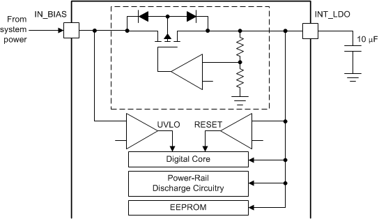
5.3.1.6 Internal LDO (INT_LDO)
The internal LDO (INT_LDO) provides a regulated voltage to the internal digital core and analog circuitry. The internal LDO has a nominal output voltage of 2.5 V and can support up to 10 mA of external load. During EEPROM programming, the output voltage is elevated to 3.6 V as described in Section 5.5.1. Therefore, any external circuitry connected to INT_LDO must be capable of supporting that voltage.
When system power fails, the UVLO comparator triggers the power-down sequence. If system power drops below 2.3 V, the digital core is reset and all remaining power rails are shut down instantaneously and are pulled low to ground by their internal discharge circuitry (DCDC1-4, and LDO1).
The internal LDO reverse blocks to prevent the discharging of the output capacitor (CINT_LDO) on the INT_LDO pin. The remaining charge on the INT_LDO output capacitor provides a supply for the power rail discharge circuitry to ensure the outputs are discharged to ground even if the system supply has failed. The amount of hold-up time specified in Section 4.5 is a function of the output capacitor value (CINT_LDO) and the amount of external load on the INT_LDO pin, if any. The design allows for enough hold-up time to sufficiently discharge DCDC1-4, and LDO1 to ensure proper processor power-down sequencing.
 Figure 5-10 Internal LDO and UVLO Sensing