ZHCSH55B December 2017 – September 2018 TPS65218D0
UNLESS OTHERWISE NOTED, this document contains PRODUCTION DATA.
- 1 器件概述
- 2 修订历史记录
- 3 Pin Configuration and Functions
- 4 Specifications
-
5 Detailed Description
- 5.1 Overview
- 5.2 Functional Block Diagram
- 5.3
Feature Description
- 5.3.1
Wake-Up and Power-Up and Power-Down Sequencing
- 5.3.1.1 Power-Up Sequencing
- 5.3.1.2 Power-Down Sequencing
- 5.3.1.3 Strobes 1 and 2
- 5.3.1.4 Supply Voltage Supervisor and Power Good (PGOOD)
- 5.3.1.5 Backup Supply Power-Good (PGOOD_BU)
- 5.3.1.6 Internal LDO (INT_LDO)
- 5.3.1.7 Current Limited Load Switches
- 5.3.1.8 LDO1
- 5.3.1.9 Coin Cell Battery Voltage Acquisition
- 5.3.1.10 UVLO
- 5.3.1.11 Power-Fail Comparator
- 5.3.1.12 Battery-Backup Supply Power-Path
- 5.3.1.13 DCDC3 / DCDC4 Power-Up Default Selection
- 5.3.1.14 I/O Configuration
- 5.3.1.15 Push Button Input (PB)
- 5.3.1.16 AC_DET Input (AC_DET)
- 5.3.1.17 Interrupt Pin (INT)
- 5.3.1.18 I2C Bus Operation
- 5.3.1
Wake-Up and Power-Up and Power-Down Sequencing
- 5.4 Device Functional Modes
- 5.5 Programming
- 5.6
Register Maps
- 5.6.1 Password Protection
- 5.6.2 Freshness Seal (FSEAL) Bit
- 5.6.3 FLAG Register
- 5.6.4
TPS65218D0 Registers
- 5.6.4.1 CHIPID Register (subaddress = 0x0) [reset = 0x5]
- 5.6.4.2 INT1 Register (subaddress = 0x1) [reset = 0x0]
- 5.6.4.3 INT2 Register (subaddress = 0x2) [reset = 0x0]
- 5.6.4.4 INT_MASK1 Register (subaddress = 0x3) [reset = 0x0]
- 5.6.4.5 INT_MASK2 Register (subaddress = 0x4) [reset = 0x0]
- 5.6.4.6 STATUS Register (subaddress = 0x5) [reset = 00XXXXXXb]
- 5.6.4.7 CONTROL Register (subaddress = 0x6) [reset = 0x0]
- 5.6.4.8 FLAG Register (subaddress = 0x7) [reset = 0x0]
- 5.6.4.9 PASSWORD Register (subaddress = 0x10) [reset = 0x0]
- 5.6.4.10 ENABLE1 Register (subaddress = 0x11) [reset = 0x0]
- 5.6.4.11 ENABLE2 Register (subaddress = 0x12) [reset = 0x0]
- 5.6.4.12 CONFIG1 Register (subaddress = 0x13) [reset = 0x4C]
- 5.6.4.13 CONFIG2 Register (subaddress = 0x14) [reset = 0xC0]
- 5.6.4.14 CONFIG3 Register (subaddress = 0x15) [reset = 0x0]
- 5.6.4.15 DCDC1 Register (offset = 0x16) [reset = 0x99]
- 5.6.4.16 DCDC2 Register (subaddress = 0x17) [reset = 0x99]
- 5.6.4.17 DCDC3 Register (subaddress = 0x18) [reset = 0x8C]
- 5.6.4.18 DCDC4 Register (subaddress = 0x19) [reset = 0xB2]
- 5.6.4.19 SLEW Register (subaddress = 0x1A) [reset = 0x6]
- 5.6.4.20 LDO1 Register (subaddress = 0x1B) [reset = 0x1F]
- 5.6.4.21 SEQ1 Register (subaddress = 0x20) [reset = 0x0]
- 5.6.4.22 SEQ2 Register (subaddress = 0x21) [reset = 0x0]
- 5.6.4.23 SEQ3 Register (subaddress = 0x22) [reset = 0x98]
- 5.6.4.24 SEQ4 Register (subaddress = 0x23) [reset = 0x75]
- 5.6.4.25 SEQ5 Register (subaddress = 0x24) [reset = 0x12]
- 5.6.4.26 SEQ6 Register (subaddress = 0x25) [reset = 0x63]
- 5.6.4.27 SEQ7 Register (subaddress = 0x26) [reset = 0x3]
- 6 Application and Implementation
- 7 Power Supply Recommendations
- 8 Layout
- 9 器件和文档支持
- 10机械、封装和可订购信息
封装选项
机械数据 (封装 | 引脚)
散热焊盘机械数据 (封装 | 引脚)
订购信息
5.3.1.12 Battery-Backup Supply Power-Path
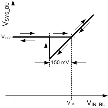
DCDC5 and DCDC6 are supplied from either the CC (coin-cell battery) input or IN_BU (main system supply). The power-path is designed to prioritize IN_BU to maximize coin-cell battery life. Whenever the PMIC is powered-up (WAIT_PWR_EN, ACTIVE, SUSPEND, RECOVERY state), the power-path is forced to select the IN_BU input. In OFF mode the power-path selects the higher of the two inputs with a built-in hysteresis of 150 mV as shown in Figure 5-17.
 Figure 5-17 Switching Behavior of the Battery-Backup-Supply Power-Path;
Power-Path Hysteresis

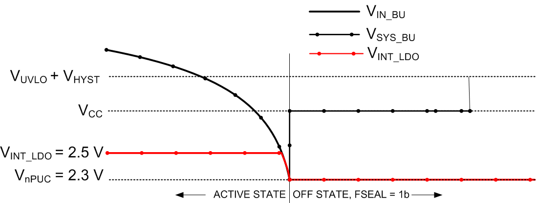
Weakening Main Battery, Strong Coin-Cell

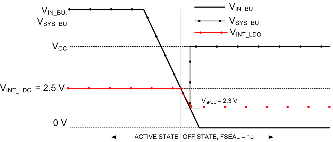
Main Power Supply Removal

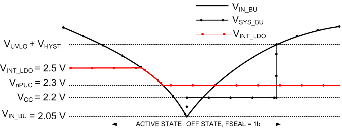
Weakening Main Battery, Weak Coin-Cell
When VIN_BIAS drops below the UVLO threshold, the PMIC shuts down all rails and enters OFF mode. At this point the power-path selects the higher of the two input supplies. If the coin-cell battery is less than 150 mV above the UVLO threshold, SYS_BU remains connected to IN_BU (see Figure 5-19). If the coin-cell is >150 mV above the UVLO threshold, the power-path switches to the CC input as shown in Figure 5-20. With no load on the main supply, the input voltage may recover over time to a value greater than the coin-cell voltage and the power-path switches back to IN_BU. This is a typical behavior in a Li-Ion battery powered system.
Depending on the system load, VIN_BIAS may drop below VINT_LDO before the power-down sequence is completed. In that case, INT_LDO is turned OFF and the digital core is reset forcing the unit into OFF mode and the power-path switches to IN_BU as shown in Figure 5-18.