ZHCSHO2G June 2010 – February 2018 TPS65251
PRODUCTION DATA.
- 1 特性
- 2 应用
- 3 说明
- 4 修订历史记录
- 5 说明 (续)
- 6 Pin Configuration and Functions
- 7 Specifications
-
8 Detailed Description
- 8.1 Overview
- 8.2 Functional Block Diagram
- 8.3
Feature Description
- 8.3.1 Adjustable Switching Frequency
- 8.3.2 Synchronization
- 8.3.3 Out-of-Phase Operation
- 8.3.4 Delayed Start-Up
- 8.3.5 Soft-Start Time
- 8.3.6 Adjusting the Output Voltage
- 8.3.7 Input Capacitor
- 8.3.8 Bootstrap Capacitor
- 8.3.9 Error Amplifier
- 8.3.10 Loop Compensation
- 8.3.11 Slope Compensation
- 8.3.12 Powergood
- 8.3.13 Current Limit Protection
- 8.3.14 Overvoltage Transient Protection
- 8.3.15 Thermal Shutdown
- 8.4 Device Functional Modes
-
9 Application and Implementation
- 9.1 Application Information
- 9.2
Typical Application
- 9.2.1 Design Requirements
- 9.2.2
Detailed Design Procedure
- 9.2.2.1 Loop Compensation Circuit
- 9.2.2.2 Selecting the Switching Frequency
- 9.2.2.3 Output Inductor Selection
- 9.2.2.4 Output Capacitor
- 9.2.2.5 Input Capacitor
- 9.2.2.6 Soft-Start Capacitor
- 9.2.2.7 Bootstrap Capacitor Selection
- 9.2.2.8 Adjustable Current Limiting Resistor Selection
- 9.2.2.9 Output Voltage and Feedback Resistors Selection
- 9.2.2.10 Compensation
- 9.2.2.11 3.3-V and 6.5-V LDO Regulators
- 9.2.3 Application Curves
- 10Power Supply Recommendations
- 11Layout
- 12器件和文档支持
- 13机械、封装和可订购信息
9.2.2.1 Loop Compensation Circuit
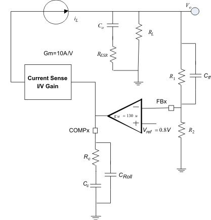
A typical compensation circuit could be type II (Rc and Cc) to have a phase margin between 60 and 90 degrees, or type III (Rc, Cc and Cff) to improve the converter transient response. CRoll adds a high frequency pole to attenuate high-frequency noise when needed. It may also prevent noise coupling from other rails if there is possibility of cross coupling in between rails when layout is very compact.
 Figure 22. Loop Compensation
To calculate the external compensation components use Table 1:
Table 1. Design Guideline for the Loop Compensation
| TYPE II CIRCUIT | TYPE III CIRCUIT | |
|---|---|---|
| Select switching frequency that is appropriate for application depending on L, C sizes, output ripple, EMI concerns and etc. Switching frequencies between 500 kHz and 1 MHz give best trade off between performance and cost. When using smaller L and Cs, switching frequency can be increased. To optimize efficiency, switching frequency can be lowered. | Type III circuit recommended for switching frequencies higher than 500 kHz. | |
| Select cross over frequency (fc) to be less than 1/5 to 1/10 of switching frequency. | Suggested
fc = fs/10 |
Suggested
fc = fs/10 |
| Set and calculate Rc. |
Equation 7.

|
Equation 8.

|
| Calculate Cc by placing a compensation zero at or before the converter dominant pole
Equation 9.

|
Equation 10.

|
Equation 11.

|
| Add CRoll if needed to remove large signal coupling to high impedance COMP node. Make sure that
Equation 12. is at least twice the cross over frequency.
|
Equation 13.

|
Equation 14.

|
| Calculate Cff compensation zero at low frequency to boost the phase margin at the crossover frequency. Make sure that the zero frequency (fzff is smaller than soft-start equivalent frequency (1/Tss). | NA |
Equation 15.

|