ZHCSHO2G June 2010 – February 2018 TPS65251
PRODUCTION DATA.
- 1 特性
- 2 应用
- 3 说明
- 4 修订历史记录
- 5 说明 (续)
- 6 Pin Configuration and Functions
- 7 Specifications
-
8 Detailed Description
- 8.1 Overview
- 8.2 Functional Block Diagram
- 8.3
Feature Description
- 8.3.1 Adjustable Switching Frequency
- 8.3.2 Synchronization
- 8.3.3 Out-of-Phase Operation
- 8.3.4 Delayed Start-Up
- 8.3.5 Soft-Start Time
- 8.3.6 Adjusting the Output Voltage
- 8.3.7 Input Capacitor
- 8.3.8 Bootstrap Capacitor
- 8.3.9 Error Amplifier
- 8.3.10 Loop Compensation
- 8.3.11 Slope Compensation
- 8.3.12 Powergood
- 8.3.13 Current Limit Protection
- 8.3.14 Overvoltage Transient Protection
- 8.3.15 Thermal Shutdown
- 8.4 Device Functional Modes
-
9 Application and Implementation
- 9.1 Application Information
- 9.2
Typical Application
- 9.2.1 Design Requirements
- 9.2.2
Detailed Design Procedure
- 9.2.2.1 Loop Compensation Circuit
- 9.2.2.2 Selecting the Switching Frequency
- 9.2.2.3 Output Inductor Selection
- 9.2.2.4 Output Capacitor
- 9.2.2.5 Input Capacitor
- 9.2.2.6 Soft-Start Capacitor
- 9.2.2.7 Bootstrap Capacitor Selection
- 9.2.2.8 Adjustable Current Limiting Resistor Selection
- 9.2.2.9 Output Voltage and Feedback Resistors Selection
- 9.2.2.10 Compensation
- 9.2.2.11 3.3-V and 6.5-V LDO Regulators
- 9.2.3 Application Curves
- 10Power Supply Recommendations
- 11Layout
- 12器件和文档支持
- 13机械、封装和可订购信息
9.2.3 Application Curves
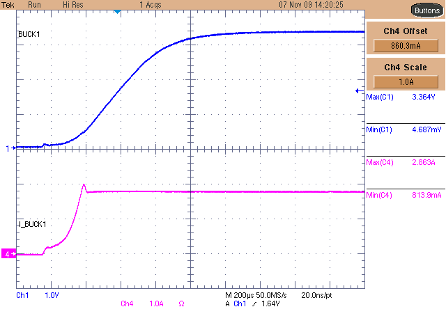 Figure 23. BUCK1 Start-Up
LO = 4.7 µH, CO = 22 µF, VOUT = 3.3 V, 2 A
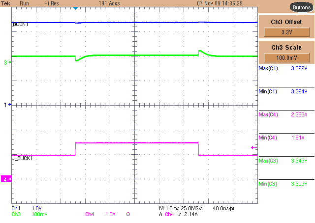 Figure 25. BUCK1 Transient Load Response
LO = 4.7 µH, CO = 22 µF, VOUT = 3.3 V, ∆I = 1 A to 1.5 A, 100 mV/div
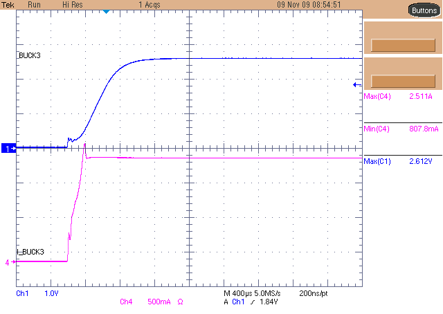 Figure 27. BUCK2 Start-Up
LO = 4.7 µH, CO = 22 µF, VOUT = 2.5 V, 1.5 A
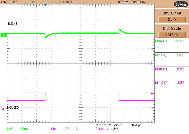 Figure 29. BUCK2 Transient Load Response
LO = 4.7 µH, CO = 22 µF, VOUT = 2.5 V, ∆I = 1 A to 1.5 A
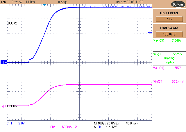 Figure 31. BUCK3 Start-Up
VOUT = 7.5 V, 0.7 A
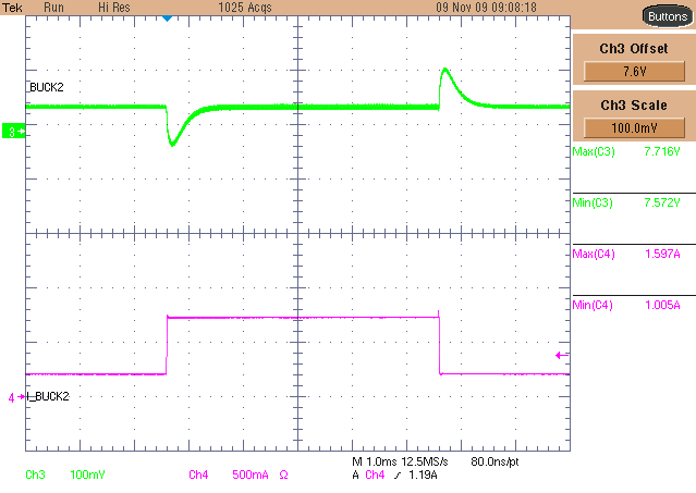 Figure 33. BUCK3 Transient Load Response
LO = 4.7 µH, CO = 22 µF, VOUT = 7.5 V, ∆I = 1 A to 1.5 A
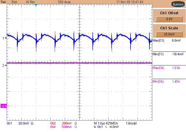 Figure 24. BUCK1 Ripple
VOUT = 3.3 V, 1.5 A, fSW = 800 kHz, 20 mV/div
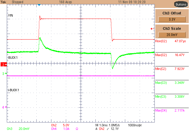 Figure 26. BUCK1 Transient Supply Response
LO = 4.7 µH, CO = 22 µF, VOUT = 3.3 V, ∆VIN = 8 V to 16.5 V, 20 mV/div
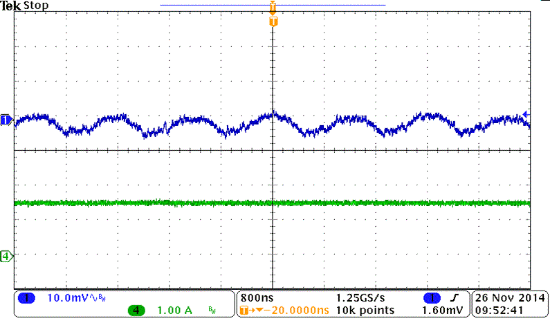
VOUT = 2.5 V, 1.5 A, fSW = 800 kHz, 10 mV/div
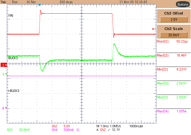 Figure 30. BUCK2 Transient Supply Response
LO = 4.7 µH, CO = 22 µF, VOUT = 2.5 V, ∆VIN = 9 V to 8 V
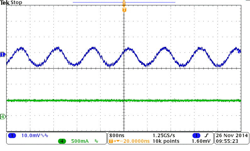 Figure 32. BUCK3 Ripple
VOUT = 7.5 V, 0.5 A, fSW = 800 kHz 10 mV/div
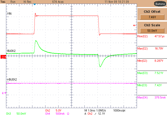 Figure 34. BUCK3 Transient Supply Response
VOUT = 2.5 V, ∆VIN = 9 V to 8 V