ZHCSBX0C december 2013 – may 2023 TPS65261 , TPS65261-1
PRODUCTION DATA
- 1
- 1 特性
- 2 应用
- 3 说明
- 4 Revision History
- 5 Pin Configuration and Functions
- 6 Specifications
-
7 Detailed Description
- 7.1 Overview
- 7.2 Functional Block Diagram
- 7.3
Feature Description
- 7.3.1 Adjusting the Output Voltage
- 7.3.2 Power Failure Detector
- 7.3.3 Enable and Adjusting Undervoltage Lockout
- 7.3.4 Soft-Start Time
- 7.3.5 Power Up Sequencing
- 7.3.6 V7V Low Dropout Regulator and Bootstrap
- 7.3.7 Out-of-Phase Operation
- 7.3.8 Output Overvoltage Protection (OVP)
- 7.3.9 Slope Compensation
- 7.3.10 Overcurrent Protection
- 7.3.11 Power Good
- 7.3.12 Adjustable Switching Frequency
- 7.3.13 Thermal Shutdown
- 7.4 Device Functional Modes
- 8 Application and Implementation
- 9 Device and Documentation Support
- 10Mechanical, Packaging, and Orderable Information
7.3.5.2 Automatic Power Sequencing
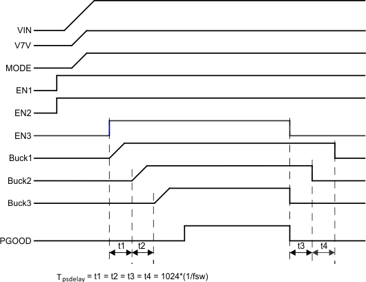
The TPS65261, TPS65261-1 starts with a pre-defined power-up and power-down sequence when the MODE pin ties high to V7V. As shown in Table 7-2, the sequence is dictated by the different combinations of EN1 and EN2 status. EN3 is used to start/stop the converters. Buck2 and buck3 are identical converters and can be swapped in the system operation to allow for additional sequencing stages. Figure 7-9 shows the power sequencing when EN1 and EN2 are pulled up high.
Table 7-2 Power Sequencing
| MODE | EN1 | EN2 | EN3 | Start Sequencing | Shutdown Sequencing | |
|---|---|---|---|---|---|---|
| Automatic Power Sequencing | High | High | High | Used to start/stop bucks in sequence | Buck1→Buck2→Buck3 | Buck3→Buck2→Buck1 |
| High | Low | High | Buck2→Buck1→Buck3 | Buck3→Buck1→Buck2 | ||
| High | High | Low | Buck2→Buck3→Buck1 | Buck1→Buck3→Buck2 | ||
| High | Low | Low | Reserved | Reserved | Reserved | |
| Externally controlled sequencing | Low | Used to start/stop buck1 | Used to start/stop buck2 | Used to start/stop buck3 | x | x |
 Figure 7-9 Automatic Power Sequencing