TA = 25°C, VIN = 12 V, VOUT1 = 1.2 V, VOUT2 = 3.3 V, VOUT3 = 1.8 V, fSW = 600 kHz (unless otherwise noted)
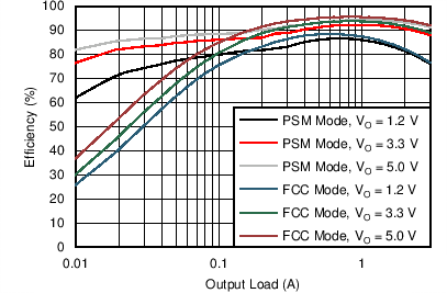 Figure 6-1 BUCK 1 Efficiency
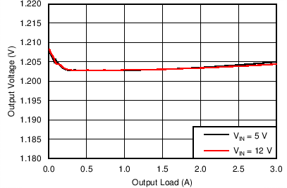 Figure 6-3 BUCK1, PSM Mode, Load Regulation
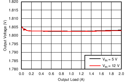 Figure 6-5 BUCK3, PSM Mode, Load Regulation
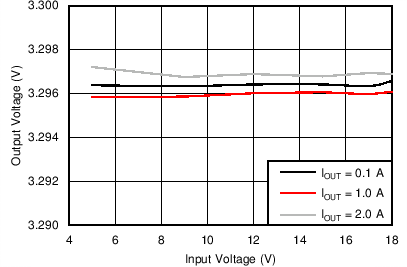 Figure 6-7 BUCK2, PSM MODE, LINE REGULATION
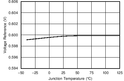 Figure 6-9 Voltage Reference vs Temperature
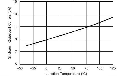 Figure 6-11 Shutdown Quiescent vs Temperature
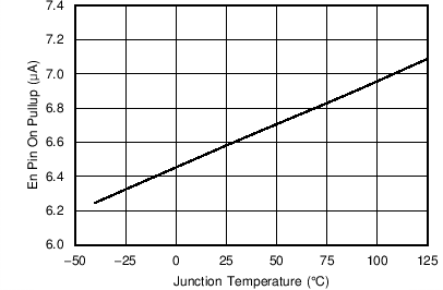 Figure 6-13 EN Pin Pullup Current vs
Temperature, EN = 1.5 V
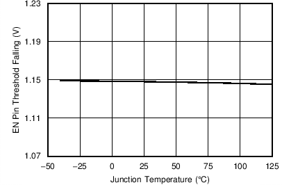 Figure 6-15 EN Pin Threshold Falling vs Temperature
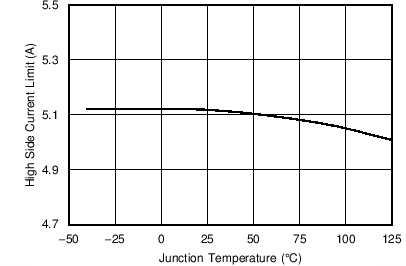 Figure 6-17 Buck1 High-Side Current Limit vs Temperature
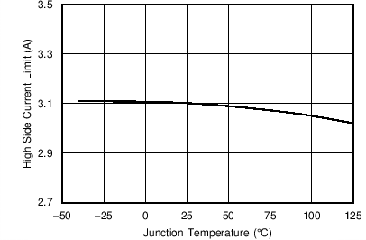 Figure 6-19 Buck3 High-Side Current Limit vs Temperature
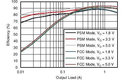 Figure 6-2 BUCK 2 Efficiency
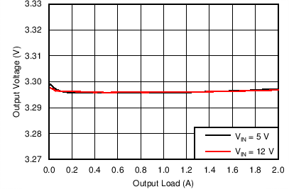 Figure 6-4 BUCK2, PSM Mode, Load Regulation
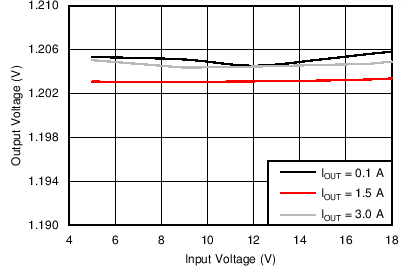 Figure 6-6 BUCK1, PSM Mode, Line Regulation
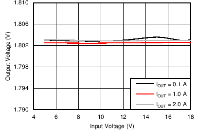 Figure 6-8 BUCK3, PSM Mode, Line Regulation
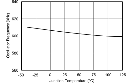 Figure 6-10 Oscillator Frequency vs Temperature
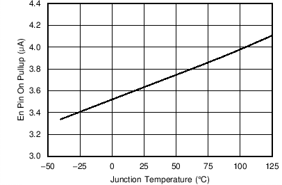 Figure 6-12 EN Pin Pull-Up Current vs Temperature, EN=1.0V
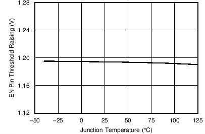 Figure 6-14 EN Pin Threshold Raising vs Temperature
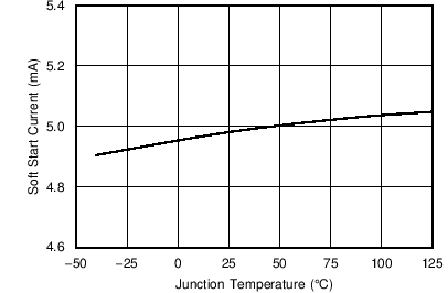 Figure 6-16 SS Pin Charge Current vs Temperature
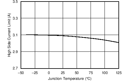 Figure 6-18 Buck2 High-Side Current Limit vs Temperature
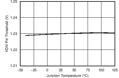 Figure 6-20 VDIV Pin Threshold vs Temperature
 Figure 6-1 BUCK 1 Efficiency


 Figure 6-9 Voltage Reference vs Temperature


 Figure 6-2 BUCK 2 Efficiency


 Figure 6-20 VDIV Pin Threshold vs Temperature