ZHCSCZ1B june 2014 – may 2023 TPS65262-1
PRODUCTION DATA
- 1
- 1 特性
- 2 应用
- 3 说明
- 4 Revision History
- 5 Device Comparison Table
- 6 Pin Configuration and Functions
- 7 Specifications
-
8 Detailed Description
- 8.1 Overview
- 8.2 Functional Block Diagram
- 8.3
Feature Description
- 8.3.1 Adjusting the Output Voltage
- 8.3.2 Enable and Adjusting UVLO
- 8.3.3 Soft-Start Time
- 8.3.4 Power-Up Sequencing
- 8.3.5 V7V Low Dropout Regulator and Bootstrap
- 8.3.6 Out-of-Phase Operation
- 8.3.7 Output Overvoltage Protection (OVP)
- 8.3.8 PSM
- 8.3.9 Slope Compensation
- 8.3.10 Overcurrent Protection (OCP)
- 8.3.11 Power Good
- 8.3.12 Thermal Shutdown
- 8.4 Device Functional Modes
- 9 Application and Implementation
- 10Device and Documentation Support
- 11Mechanical, Packaging, and Orderable Information
8.3.4.1 External Power Sequencing
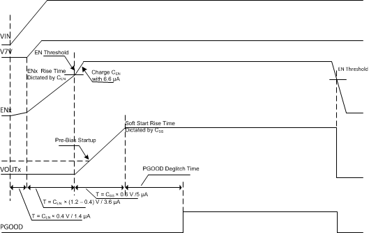
The TPS65262-1 has a dedicated enable pin for each converter. The converter enable pins are biased by a current source that allows for easy sequencing with the addition of an external capacitor. Disabling the converter with an active pulldown transistor on the ENx pin allows for a predictable power-down timing operation. Figure 8-3 shows the timing diagram of a typical buck power-up sequence with a capacitor connected at ENx pin.
A typical 1.4-µA current charges the ENx pin from the input supply when the ENx pin voltage is lower than typical 0.4 V. The internal V7V LDO turns on when the ENx pin voltage rises to typical 0.4 V and a 3.6-µA pullup current sources ENx. After the ENx pin voltage reaches 1.2 V typical, 3-µA hysteresis current sources to the pin to improve noise sensitivity. If all output voltages are in regulation, PGOOD is asserted after PGOOD deglitch time.
 Figure 8-3 Startup Power Sequence