ZHCSCL5D january   2014  – may 2023 TPS65262

PRODUCTION DATA  

  1.   1
  2. 特性
  3. 应用
  4. 说明
  5. Revision History
  6. Pin Configuration and Functions
  7. Specifications
    1. 6.1 Absolute Maximum Ratings
    2. 6.2 ESD Ratings
    3. 6.3 Recommended Operating Conditions
    4. 6.4 Thermal Information
    5. 6.5 Electrical Characteristics
    6. 6.6 Typical Characteristics
  8. Detailed Description
    1. 7.1 Overview
    2. 7.2 Functional Block Diagram
    3. 7.3 Feature Description
      1. 7.3.1  Adjusting the Output Voltage
      2. 7.3.2  Enable and Adjusting Undervoltage Lockout
      3. 7.3.3  Soft-Start Time
      4. 7.3.4  Power-Up Sequencing
        1. 7.3.4.1 External Power Sequencing
        2. 7.3.4.2 Automatic Power Sequencing
      5. 7.3.5  V7V Low Dropout Regulator and Bootstrap
      6. 7.3.6  Out-of-Phase Operation
      7. 7.3.7  Output Overvoltage Protection (OVP)
      8. 7.3.8  PSM
      9. 7.3.9  Slope Compensation
      10. 7.3.10 Overcurrent Protection
        1. 7.3.10.1 High-Side MOSFET Overcurrent Protection
        2. 7.3.10.2 Low-Side MOSFET Overcurrent Protection
      11. 7.3.11 Power Good
      12. 7.3.12 Thermal Shutdown
    4. 7.4 Device Functional Modes
      1. 7.4.1 Operation With VIN < 4.5 V (Minimum VIN)
      2. 7.4.2 Operation With EN Control
      3. 7.4.3 Operation at Light Loads
  9. Application and Implementation
    1. 8.1 Application Information
    2. 8.2 Typical Application
      1. 8.2.1 Design Requirements
      2. 8.2.2 Detailed Design Procedure
        1. 8.2.2.1 Output Inductor Selection
        2. 8.2.2.2 Output Capacitor Selection
        3. 8.2.2.3 Input Capacitor Selection
        4. 8.2.2.4 Loop Compensation
      3. 8.2.3 Application Curves
    3. 8.3 Power Supply Recommendations
    4. 8.4 Layout
      1. 8.4.1 Layout Guidelines
      2. 8.4.2 Layout Example
  10. Device and Documentation Support
    1. 9.1 接收文档更新通知
    2. 9.2 支持资源
    3. 9.3 Trademarks
    4. 9.4 静电放电警告
    5. 9.5 术语表
  11. 10Mechanical, Packaging, and Orderable Information

封装选项

机械数据 (封装 | 引脚)
散热焊盘机械数据 (封装 | 引脚)
订购信息

Typical Characteristics

TA = 25°C, VIN = 12 V, VOUT1 = 1.2 V, VOUT2 = 1.8 V, VOUT3 = 3.3 V, ƒSW = 600 kHz (unless otherwise noted)
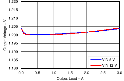
GUID-E7454FAD-DCA9-44F3-93B0-90488F8B5F02-low.png
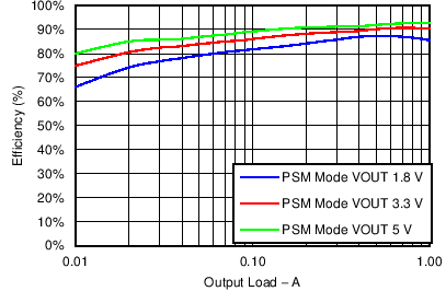
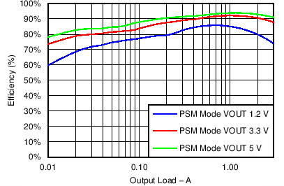
Figure 6-1 Buck1 Efficiency
GUID-7FEC2834-CDFE-4810-ADA0-A8F4BBC18E8C-low.png
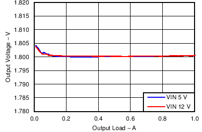
Figure 6-3 Buck1, Load Regulation
GUID-510DB435-BD87-4EEB-9591-B9251E1D1741-low.png
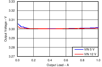
Figure 6-5 Buck3, Load Regulation
GUID-8B819B08-7FC6-4591-AE69-1C9FBFAF2274-low.png
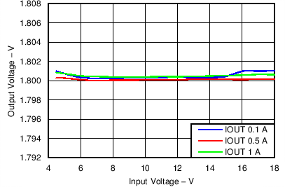
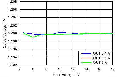
Figure 6-7 Buck2, Line Regulation
GUID-3C74C02C-2232-4A13-B958-212D97F8967F-low.png
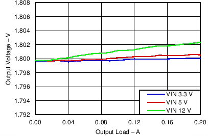
Figure 6-9 LDO1, Load Regulation
GUID-21998A0E-4247-48D8-855A-FCF516343DF0-low.png
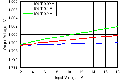
Figure 6-11 LDO1, Line Regulation
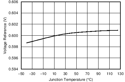
GUID-08E591AF-2019-4050-9081-17727A6A0D39-low.png
Figure 6-13 Voltage Reference vs Temperature
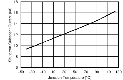
GUID-0DB2B082-FC90-472A-AA85-5F0F9EA248BA-low.png
Figure 6-15 Shutdown Quiescent Current vs Temperature
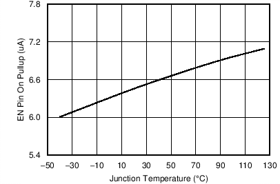
GUID-105D8D43-4063-47CE-9FC2-0696C5E7D692-low.png
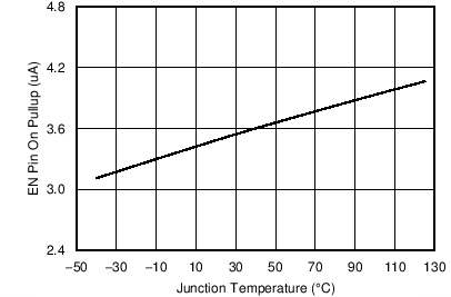
Figure 6-17 EN Pin Pullup Current vs Temperature, EN = 1.5 V
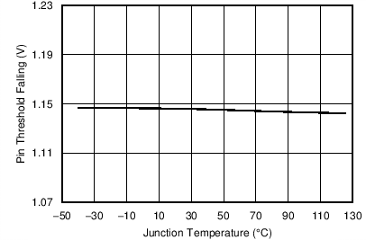
GUID-9034D235-C6F6-4088-84BC-67245D3A6B16-low.png
Figure 6-19 EN Pin Threshold Falling vs Temperature
GUID-CDC712FF-D834-4C09-9E94-C6A07C2D3D55-low.png
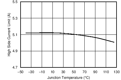
Figure 6-21 Buck1 High-Side Current Limit vs Temperature
GUID-61FD5191-847E-4838-9C0F-54B6EFDB96F6-low.png
Figure 6-2 Buck2 Efficiency
GUID-52F3FF6D-69B6-4045-A193-4CB082CD9FFA-low.png
Figure 6-4 Buck2, Load Regulation
GUID-A2ABD389-AEAD-4F0C-AD9A-ABB7B59FB5C5-low.png
Figure 6-6 Buck1, Line Regulation
GUID-A5978751-2648-4C97-9E7A-175124CE1800-low.png
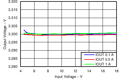
Figure 6-8 Buck3, Line Regulation
GUID-8F66B89E-76D5-41A0-B8A8-97EA8F61CB37-low.png
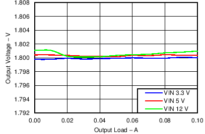
Figure 6-10 LDO2, Load Regulation
GUID-1BCCF0D1-4580-4AD3-8496-6A0F8B2236A2-low.png
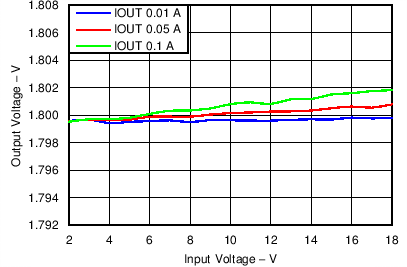
Figure 6-12 LDO2, Line Regulation
GUID-194823F0-28EE-4A65-B7A4-44CD8AF05562-low.png
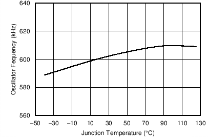
Figure 6-14 Oscillator Frequency vs Temperature
GUID-485FBF6F-2DE6-4EBB-8006-D4FC84F360B5-low.png
Figure 6-16 EN Pin Pullup Current vs Temperature, EN = 1 V
GUID-686327B3-6B67-4760-A9F8-841BE699DAB3-low.png
Figure 6-18 EN Pin Threshold Rising vs Temperature
GUID-6CF02DF3-8F59-4D8E-B80E-6BE38B041A95-low.png
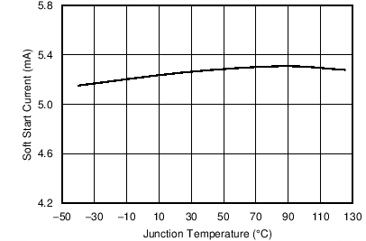
Figure 6-20 SS Pin Charge Current vs Temperature
GUID-59296FDF-9F85-4642-B285-0AFEA9ECA28D-low.png
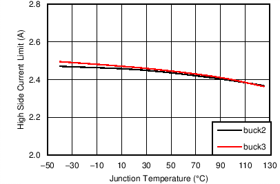
Figure 6-22 Buck2, 3 High-Side Current Limit vs Temperature