ZHCSG38A March 2017 – November 2022 TPS65263-1Q1
PRODUCTION DATA
- 1 特性
- 2 应用
- 3 说明
- 4 Revision History
- 5 Pin Configuration and Functions
- 6 Specifications
-
7 Detailed Description
- 7.1 Overview
- 7.2 Functional Block Diagram
- 7.3
Feature Description
- 7.3.1 Adjusting the Output Voltage
- 7.3.2 Enable and Adjusting UVLO
- 7.3.3 Soft-Start Time
- 7.3.4 Power-Up Sequencing
- 7.3.5 V7V Low-Dropout Regulator and Bootstrap
- 7.3.6 Out-of-Phase Operation
- 7.3.7 Output Overvoltage Protection (OVP)
- 7.3.8 PSM
- 7.3.9 Slope Compensation
- 7.3.10 Overcurrent Protection
- 7.3.11 Power Good
- 7.3.12 Thermal Shutdown
- 7.4 Device Functional Modes
- 7.5 Register Maps
- 8 Application and Implementation
- 9 Device and Documentation Support
- 10Mechanical, Packaging, and Orderable Information
7.3.10.2 Low-Side MOSFET Overcurrent Protection
While the low-side MOSFET is turned on, its conduction current is monitored by the internal circuitry. During normal operation, the low-side MOSFET sources current to the load. At the end of every clock cycle, the low-side MOSFET sourcing current is compared to the internally set low-side sourcing current limit. If the low-side sourcing current is exceeded, the high-side MOSFET is not turned on and the low-side MOSFET stays on for the next cycle. The high-side MOSFET is turned on again when the low-side current is below the low-side sourcing current limit at the start of a cycle.
The low-side MOSFET can also sink current from the load. If the low-side sinking current limit is exceeded, the low-side MOSFET is turned off immediately for the rest of that clock cycle. In this scenario both MOSFETs are off until the start of the next cycle.
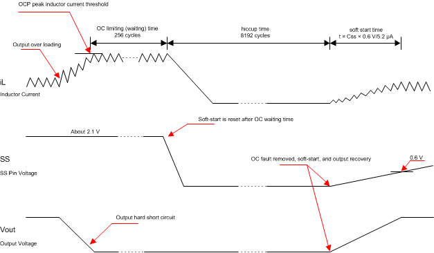
Furthermore, if an output overload condition (as measured by the COMP pin voltage) has lasted for more than the hiccup wait time which is programmed for 256 switching cycles shown in Figure 7-11, the device shuts down and restarts after the hiccup time of 8192 cycles. The hiccup mode helps to reduce the device power dissipation under severe overcurrent condition.
 Figure 7-11 Overcurrent Protection