ZHCSBF7C August 2013 – May 2015 TPS65279
PRODUCTION DATA.
- 1 特性
- 2 应用范围
- 3 说明
- 4 修订历史记录
- 5 说明(续)
- 6 Pin Configuration and Functions
- 7 Specifications
-
8 Detailed Description
- 8.1 Overview
- 8.2 Functional Block Diagram
- 8.3
Feature Description
- 8.3.1 Enable and Adjusting Undervoltage Lockout (UVLO)
- 8.3.2 Adjustable Switching Frequency and Synchronization
- 8.3.3 Soft-Start Time
- 8.3.4 Out-of-Phase Operation
- 8.3.5 Output Overvoltage Protection (OVP)
- 8.3.6 Bootstrap Voltage (BOOT) and Low Dropout Operation
- 8.3.7 Overcurrent Protection
- 8.3.8 Current Sharing Operation
- 8.3.9 Thermal Shutdown
- 8.4 Device Functional Modes
- 9 Application and Implementation
- 10Power Supply Recommendations
- 11Layout
- 12器件和文档支持
- 13机械、封装和可订购信息
封装选项
机械数据 (封装 | 引脚)
散热焊盘机械数据 (封装 | 引脚)
订购信息
11 Layout
11.1 Layout Guidelines
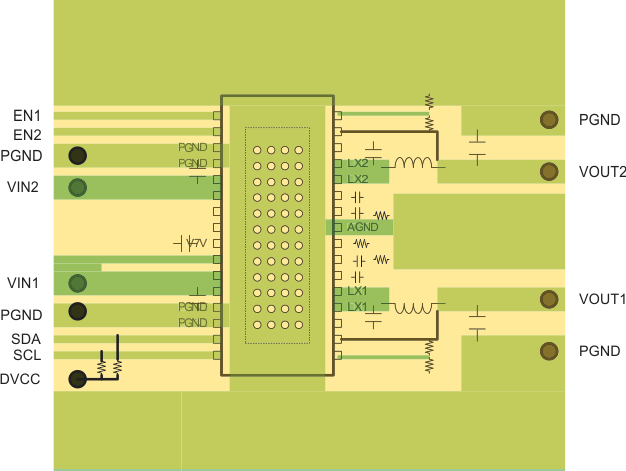
The designer can layout the TPS65279 on a 2-layer PCB as shown in Figure 46.
Layout is a critical portion of good power supply design. See Figure 46 for a PCB layout example. The top layer contains the main power traces for VIN, VOUT, and VLX. Also on the top layer are connections for the remaining pins of the TPS65279 and a large top side area filled with ground. The top layer ground area should be connected to the internal ground layer(s) using vias at the input bypass capacitor, the output filter capacitor and directly under the TPS65279 device to provide a thermal path from the exposed thermal pad land to ground. The bottom layer acts as ground plane connecting analog ground and power ground.
The GND pin should be tied directly to the power pad under the IC and the power pad. For operation at full rated load, the top side ground area together with the internal ground plane, must provide adequate heat dissipating area. There are several signals paths that conduct fast changing currents or voltages that can interact with stray inductance or parasitic capacitance to generate noise or degrade the power supplies performance. To help eliminate these problems, the PVIN pin should be bypassed to ground with a low ESR ceramic bypass capacitor with X5R or X7R dielectric. Take care to minimize the loop area formed by the bypass capacitor connections, the PVIN pins, and the ground connections.
The VIN pin must also be bypassed to ground using a low ESR ceramic capacitor with X5R or X7R dielectric.
Since the LX connection is the switching node, the output inductor should be located close to the LX pins, and the area of the PCB conductor minimized to prevent excessive capacitive coupling. The output filter capacitor ground should use the same power ground trace as the PVIN input bypass capacitor. Try to minimize this conductor length while maintaining adequate width. The additional external components can be placed approximately as shown.
11.2 Layout Example
 Figure 46. TPS65279 Layout on 2-Layer PCB