ZHCSBF7C August 2013 – May 2015 TPS65279
PRODUCTION DATA.
- 1 特性
- 2 应用范围
- 3 说明
- 4 修订历史记录
- 5 说明(续)
- 6 Pin Configuration and Functions
- 7 Specifications
-
8 Detailed Description
- 8.1 Overview
- 8.2 Functional Block Diagram
- 8.3
Feature Description
- 8.3.1 Enable and Adjusting Undervoltage Lockout (UVLO)
- 8.3.2 Adjustable Switching Frequency and Synchronization
- 8.3.3 Soft-Start Time
- 8.3.4 Out-of-Phase Operation
- 8.3.5 Output Overvoltage Protection (OVP)
- 8.3.6 Bootstrap Voltage (BOOT) and Low Dropout Operation
- 8.3.7 Overcurrent Protection
- 8.3.8 Current Sharing Operation
- 8.3.9 Thermal Shutdown
- 8.4 Device Functional Modes
- 9 Application and Implementation
- 10Power Supply Recommendations
- 11Layout
- 12器件和文档支持
- 13机械、封装和可订购信息
封装选项
机械数据 (封装 | 引脚)
散热焊盘机械数据 (封装 | 引脚)
订购信息
8 Detailed Description
8.1 Overview
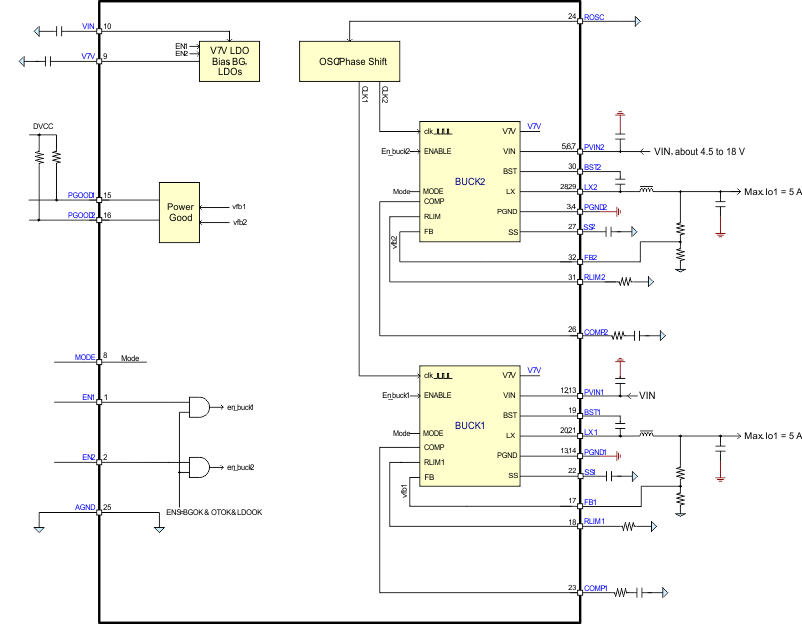
TPS65279 is a dual 5-A/5-A output current, synchronous step-down (buck) converter with integrated
N-channel MOSFETs. A wide 4.5-V to 18-V input supply range to buck encompasses most intermediate bus voltages operating off 9-V, 12-V or 15-V power bus.
TPS65279 implements a constant frequency, peak current mode control which simplifies external frequency compensation. The wide switching frequency of 200 kHz to 1600 kHz allows for efficiency and size optimization when selecting the output filter components. The switching frequency can be adjusted with an external resistor to ground on the ROSC pin. The TPS65279 also has an internal phase lock loop (PLL) controlled by the ROSC pin that can be used to synchronize the switching cycle to the falling edge of an external system clock. 180° out-of-phase operation between two channels reduces input filter and power supply induced noise.
TPS65279 has been designed for safe monotonic startup into prebiased loads. The default start up is typically 4.5 V. The EN pin has an internal pullup current source that can be used to adjust the input voltage under voltage lockout (UVLO) with two external resistors. In addition, the EN pin can be floating for automatically starting up the TPS65279 with the internal pullup current.
The integrated MOSFETs of each channel allow for high efficiency power supply designs with continuous output currents up to 5 A. The MOSFETs have been sized to optimize efficiency for lower duty cycle applications.
The TPS65279 reduces the external component count by integrating the boot recharge circuit. The bias voltage for the integrated high-side MOSFET is supplied by a capacitor between the BOOT and LX pins. The boot capacitor voltage is monitored by a BOOT to LX UVLO (BOOT-LX UVLO) circuit allowing LX pin to be pulled low to recharge the boot capacitor. The TPS65279 can operate at 100% duty cycle as long as the boot capacitor voltage is higher than the preset BOOT-LX UVLO threshold which is typically 2.1 V.
The TPS65279 has a power good comparator with hysteresis which monitors the output voltage through internal feedback voltage.
The SS (soft start/tracking) pin is used to minimize inrush current or provide power supply sequencing during power up. A small value capacitor or resistor divider should be coupled to the pin for soft start or critical power supply sequencing requirements.
The TPS65279 is protected from output overvoltage, overload, and thermal fault conditions. The TPS65279 minimizes excessive output overvoltage transients by taking advantage of the power good comparator. When the overvoltage comparator is activated, the high-side MOSFET is turned off and prevented from turning on until the internal feedback voltage is lower than 107.5% of the 0.6-V reference voltage. The TPS65279 implements both high-side MOSFET overload protection and bidirectional low-side MOSFET overload protections which help control the inductor current and avoid current runaway. If the over current condition has lasted for more than the hiccup wait time, the TPS65279 will shut down and re-start after the hiccup time. The TPS65279 also shuts down if the junction temperature is higher than thermal shutdown trip point. When the junction temperature drops 20°C typically below the thermal shutdown trip point, the built-in thermal shutdown hiccup timer is triggered. The TPS65279 will be restarted under control of the soft start circuit automatically after the thermal shutdown hiccup time is over.
Furthermore, if the over-current condition has lasted for more than the hiccup wait time which is programmed for 512 switching cycles, the TPS65279 will shut down itself and restart after the hiccup time which is set for 16384 cycles. The hiccup mode helps to reduce the device power dissipation under severe over-current conditions.
The TPS65279 operates at any load conditions unless the COMP pin voltage drops below the COMP pin start switching threshold which is typically 0.25 V.
When PSM mode operation is enabled, the TPS65279 monitors the peak switch current of the high-side MOSFET. Once the peak switch current is lower than typically 1 A, the device stops switching to boost the efficiency until the peak switch current is higher than typically 1 A again.
8.3 Feature Description
8.3.1 Enable and Adjusting Undervoltage Lockout (UVLO)
The EN pin provides electrical on/off control of the device. Once the EN pin voltage exceeds the threshold voltage, the device starts operation. If the EN pin voltage is pulled below the threshold voltage, the regulator stops switching and enters low Iq state.
The EN pin has an internal pullup current source, allowing the user to float the EN pin for enabling the device. If an application requires controlling the EN pin, use open drain or open collector output logic to interface with the pin.
The device implements internal UVLO circuitry on the VIN pin. The device is disabled when the VIN pin voltage falls below the internal VIN UVLO threshold. The internal VIN UVLO threshold has a hysteresis of 500 mV.
8.3.2 Adjustable Switching Frequency and Synchronization
The ROSC pin can be used to set the switching frequency of the device in two mode. The resistor mode is to connect a resistor between ROSC pin and GND. The switching frequency of the device is adjustable from 200 kHz to 1600 kHz. The other mode called synchronization mode is to connect an external clock signal directly to the ROSC pin. The device is synchronized to the external clock frequency with PLL.
Synchronization mode overrides the resistor mode. The device is able to detect the proper mode automatically and switch from synchronization mode to resistor mode.
8.3.2.1 Synchronization
An internal phase locked loop (PLL) has been implemented to allow synchronization between 200 kHz and 1600 kHz, and to easily switch from Resistor mode to Synchronization mode.
To implement the synchronization feature, connect a square wave clock signal to the ROSC pin with a duty cycle between 20% to 80%. The clock signal amplitude must transition lower than 0.8 V and higher than 2 V. The start of the switching cycle is synchronized to the falling edge of ROSC pin.
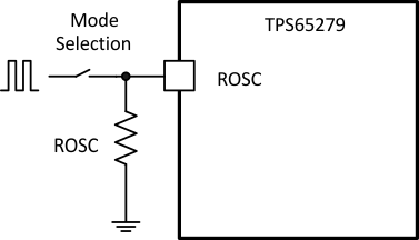
In applications where both Resistor mode and Synchronization mode are needed, the device can be configured as shown in Figure 17. Before the external clock is present, the device works in Resistor mode and the switching frequency is set by ROSC resistor. When the external clock is present, the Synchronization mode overrides the Resistor mode. The first time the ROSC pin is pulled above the ROSC high threshold (2 V), the device switches from the Resistor mode to the Synchronization mode and the ROSC pin becomes high impedance as the PLL starts to lock onto the frequency of the external clock. It is not recommended to switch from the Synchronization mode back to the Resistor mode because the internal switching frequency drops to 100 kHz first before returning to the switching frequency set by ROSC resistor.
 Figure 17. Resistor Mode and Synchronization Mode
8.3.3 Soft-Start Time
The start-up of buck output is controlled by the voltage on the respective SS pin. When the voltage on the SS pin is less than the internal 0.6-V reference, the TPS65279 regulates the internal feedback voltage to the voltage on the SS pin instead of 0.6 V. The SS pin can be used to program an external soft-start function or to allow output of buck to track another supply during start-up. The device has an internal pullup current source of 6 µA that charges an external soft-start capacitor to provide a linear ramping voltage at SS pin. The TPS65279 regulates the internal feedback voltage according to the voltage on the SS pin, allowing VOUT to rise smoothly from 0 V to its final regulated voltage. The total soft-start time will be calculated approximately:

8.3.4 Out-of-Phase Operation
In order to reduce input ripple current, Buck 1 and Buck 2 operate 180° out-of-phase. This enables the system having less input ripple, then to lower component cost, save board space and reduce EMI.
8.3.5 Output Overvoltage Protection (OVP)
The device incorporates an output overvoltage protection (OVP) circuit to minimize output voltage overshoot. For example, when the power supply output is overloaded the error amplifier compares the actual output voltage to the internal reference voltage. If the FB pin voltage is lower than the internal reference voltage for a considerable time, the output of the error amplifier demands maximum output current. Once the condition is removed, the regulator output rises and the error amplifier output transitions to the steady state voltage. In some applications with small output capacitance, the power supply output voltage can respond faster than the error amplifier. This leads to the possibility of an output overshoot. The OVP feature minimizes the overshoot by comparing the FB pin voltage to the OVP threshold. If the FB pin voltage is greater than the OVP threshold the high-side MOSFET is turned off preventing current from flowing to the output and minimizing output overshoot. When the FB voltage drops lower than the OVP threshold, the high-side MOSFET is allowed to turn on at the next clock cycle.
8.3.6 Bootstrap Voltage (BOOT) and Low Dropout Operation
The device has an integrated boot regulator, and requires a small ceramic capacitor between the BOOT and LX pins to provide the gate drive voltage for the high-side MOSFET. The boot capacitor is charged when the BOOT pin voltage is less than VIN and BOOT-LX voltage is below regulation. The value of this ceramic capacitor should be 0.1 μF. A ceramic capacitor with an X7R or X5R grade dielectric with a voltage rating of 10 V or higher is recommended because of the stable characteristics over temperature and voltage.
To improve drop out, the device is designed to operate at 100% duty cycle as long as the BOOT to LX pin voltage is greater than the BOOT-LX UVLO threshold which is typically 2.1 V. When the voltage between BOOT and LX drops below the BOOT-LX UVLO threshold the high-side MOSFET is turned off and the low-side MOSFET is turned on allowing the boot capacitor to be recharged. In applications with split input voltage rails, 100% duty cycle operation can be achieved as long as (VIN – PVIN) > 4 V.
8.3.7 Overcurrent Protection
The device is protected from over current conditions by cycle-by-cycle current limiting on both the high-side MOSFET and the low-side MOSFET.
8.3.7.1 High-Side MOSFET Overcurrent Protection
The device implements current mode control which uses the COMP pin voltage to control the turn off of the high-side MOSFET and the turn on of the low-side MOSFET on a cycle by cycle basis. Each cycle the switch current and the current reference generated by the COMP pin voltage are compared, when the peak switch current intersects the current reference the high-side switch is turned off.
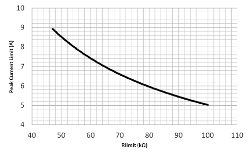
TPS65279 features adjustable overcurrent protection trip point. The peak current limit can be set by external resistors connected between pin RLIM1/2 to ground. By setting lower current limit, lower current rating inductor can be used to reduce system cost.
 Figure 18. Peak Current Limit vs Rlimit
8.3.7.2 Low-Side MOSFET Overcurrent Protection
While the low-side MOSFET is turned on its conduction current is monitored by the internal circuitry. During normal operation the low-side MOSFET sources current to the load. At the end of every clock cycle, the low-side MOSFET sourcing current is compared to the internally set low-side sourcing current limit. If the low-side sourcing current is exceeded, the high-side MOSFET is not turned on and the low-side MOSFET stays on for the next cycle. The high-side MOSFET is turned on again when the low-side current is below the low-side sourcing current limit at the start of a cycle.
The low-side MOSFET may also sink current from the load. If the low-side sinking current limit is exceeded the low-side MOSFET is turned off immediately for the rest of that clock cycle. In this scenario both MOSFETs are off until the start of the next cycle.
Furthermore, if an output overload condition (as measured by the COMP pin voltage) has lasted for more than the hiccup wait time which is programmed for 512 switching cycles, the device will shut down itself and restart after the hiccup time of 16384 cycles. The hiccup mode helps to reduce the device power dissipation under severe overcurrent conditions. When one channel is in OCP, the other channel is not impacted and remains independent.
8.3.8 Current Sharing Operation
As TPS65279 uses peak current mode control method, the two buck converters can be paralleled together to provide large current. Paralleling two bucks provides some advantages over single buck operation, such as smaller input and output ripple, faster response in load transient, and so forth. The converters will work in current sharing mode by connecting the iShare pin to high. Once in current mode, signal pins in Buck 2 are not active, for example, FB2, COMP2, SS2, these pins will be neglected. Connecting FB2 to GND and floating COMP2, SS2, PGOOD2 are recommended.
8.3.9 Thermal Shutdown
The internal thermal shutdown circuitry forces the device to stop switching if the junction temperature exceeds 160°C typically. Once the junction temperature drops below 140°C typically, the internal thermal hiccup timer will start to count. The device reinitiates the power up sequence after the built-in thermal shutdown hiccup time (16384 cycles) is over.
8.4 Device Functional Modes
8.4.1 CCM Operation Mode
When the VIN/PVINx are above UVLO threshold and ENx are above the threshold, two switchers operate in continuous current mode(CCM) when MODE pin connects to GND. In CCM, the converters work in peak current mode for easy loop compensation and cycle-by-cycle high side MOSFET current limit.
8.4.2 PSM Operation Mode
When connect MODE pin to V7V, PSM mode is enabled. The devices are designed to operate in high-efficiency PSM under light load conditions. Pulse skipping is initiated when the switch current falls to 0 A. During pulse skipping, the low-side FET is turned off when the switch current falls to 0 A. The switching node (LX) waveform takes on the characteristics of DCM operation and the apparent switching frequency decreases.
8.4.3 Current Sharing Mode
When ISHARE pin connects to high, SW1/SW2 pair output are shared, the responding pairs current sharing mode is enabled and the two buck converters are paralleled together to provide large current. For the detail configuration, see current sharing application schematics.
