ZHCSJF4 February   2019 TPS65295

PRODUCTION DATA.  

  1. 特性
  2. 应用
  3. 说明
    1.     典型应用
  4. 修订历史记录
  5. Pin Configuration and Functions
    1.     Pin Functions
  6. Specifications
    1. 6.1 Absolute Maximum Ratings
    2. 6.2 ESD Ratings
    3. 6.3 Recommended Operating Conditions
    4. 6.4 Thermal Information
    5. 6.5 Electrical Characteristics
    6. 6.6 Typical Characteristics
  7. Detailed Description
    1. 7.1 Overview
    2. 7.2 Functional Block Diagram
    3. 7.3 Feature Description
      1. 7.3.1 PWM Operation and D-CAP3 Control
      2. 7.3.2 Advanced Eco-mode Control
      3. 7.3.3 Soft Start and Prebiased Soft Start
      4. 7.3.4 Power Good
      5. 7.3.5 Overcurrent Protection and Undervoltage Protection
      6. 7.3.6 Overvoltage Protection
      7. 7.3.7 UVLO Protection
      8. 7.3.8 Output Voltage Discharge
      9. 7.3.9 Thermal Shutdown
    4. 7.4 Device Functional Modes
      1. 7.4.1 Light Load Operation for VDDQ Buck and VPP Buck
      2. 7.4.2 Output State Control
      3. 7.4.3 Output Sequence Control
  8. Application and Implementation
    1. 8.1 Application Information
    2. 8.2 Typical Application
      1. 8.2.1 Design Requirements
      2. 8.2.2 Detailed Design Procedure
        1. 8.2.2.1 External Component Selection
          1. 8.2.2.1.1 Inductor Selection
          2. 8.2.2.1.2 Output Capacitor Selection
          3. 8.2.2.1.3 Input Capacitor Selection
          4. 8.2.2.1.4 Bootstrap Capacitor and Resistor Selection
      3. 8.2.3 Application Curves
  9. Power Supply Recommendations
  10. 10Layout
    1. 10.1 Layout Guidelines
    2. 10.2 Layout Example
  11. 11器件和文档支持
    1. 11.1 器件支持
      1. 11.1.1 第三方米6体育平台手机版_好二三四免责声明
    2. 11.2 接收文档更新通知
    3. 11.3 社区资源
    4. 11.4 商标
    5. 11.5 静电放电警告
    6. 11.6 术语表
  12. 12机械、封装和可订购信息
    1. 12.1 Package Option Addendum
      1. 12.1.1 Packaging Information
      2. 12.1.2 Tape and Reel Information

封装选项

机械数据 (封装 | 引脚)
散热焊盘机械数据 (封装 | 引脚)
订购信息

Output Sequence Control

There are specific sequencing requirements for the DDR4 VDDQ and VPP rails. The TPS65295 follows the DDR4 power rail sequence requirements as shown in Figure 29 and Figure 30. VPP is greater than VDDQ at all times during ramp up, operating, and ramp down. The VTT output ramp and stable within 35 µs after VTT_CNTL asserted.
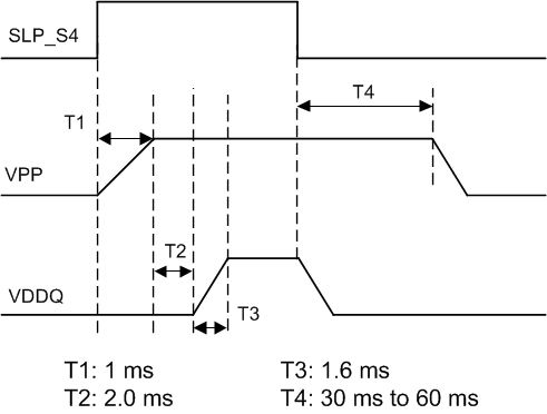
TPS65295 timing-v02-slvsek000.gifFigure 29. Power Sequence, VPP and VDDQ vs SLP_S4
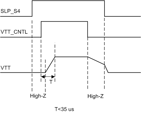
TPS65295 timing-02-slvsek0.gifFigure 30. Power Sequence, VTT vs VTT_CNTL