ZHCSL05C October 2019 – October 2023 TPS65313-Q1
PRODUCTION DATA
- 1
- 1 特性
- 2 应用
- 3 说明
- 4 器件功能方框图
- 5 Revision History
- 6 说明(续)
- 7 Device Option Table
- 8 Pin Configuration and Functions
-
9 Specifications
- 9.1 Absolute Maximum Ratings
- 9.2 ESD Ratings
- 9.3 Recommended Operating Conditions
- 9.4 Thermal Information
- 9.5 Power-On-Reset, Current Consumption, and State Timeout Characteristics
- 9.6 PLL/Oscillator and SYNC_IN Pin Characteristics
- 9.7 Wide-VIN Synchronous Buck Regulator (Wide-VIN BUCK) Characteristics
- 9.8 Low-Voltage Synchronous Buck Regulator (LV BUCK) Characteristics
- 9.9 Synchronous Boost Converter (BOOST) Characteristics
- 9.10 Internal Voltage Regulator (VREG) Characteristics
- 9.11 Voltage Monitors for Regulators Characteristics
- 9.12 External General Purpose Voltage Monitor Characteristics
- 9.13 VIN and VIN_SAFE Under-Voltage and Over-Voltage Warning Characteristics
- 9.14 WAKE Input Characteristics
- 9.15 NRES (nRESET) Output Characteristics
- 9.16 ENDRV/nIRQ Output Characteristics
- 9.17 Analog DIAG_OUT
- 9.18 Digital INPUT/OUTPUT IOs (SPI Interface IOs, DIAG_OUT/SYNC_OUT, MCU_ERROR)
- 9.19 BUCK1, BUCK2, BOOST Thermal Shutdown / Over Temperature Protection Characteristics
- 9.20 PGNDx Loss Detection Characteristics
- 9.21 SPI Timing Requirements
- 9.22 SPI Characteristics
- 9.23 Typical Characteristics
- 10Parameter Measurement Information
-
11Detailed Description
- 11.1 Overview
- 11.2 Functional Block Diagram
- 11.3
Wide-VIN Buck Regulator (BUCK1)
- 11.3.1 Fixed-Frequency Voltage-Mode Step-Down Regulator
- 11.3.2 Operation
- 11.3.3 Voltage Monitoring (Monitoring and Protection)
- 11.3.4 Overcurrent Protection (Monitoring and Protection)
- 11.3.5 Thermal Warning and Shutdown Protection (Monitoring and Protection)
- 11.3.6 Overvoltage Protection (OVP) (Monitoring and Protection)
- 11.3.7 Extreme Overvoltage Protection (EOVP) (Monitoring and Protection)
- 11.4
Low-Voltage Buck Regulator (BUCK2)
- 11.4.1 Fixed-Frequency Peak-Current Mode Step-Down Regulator
- 11.4.2 Operation
- 11.4.3 Output Voltage Monitoring (Monitoring and Protection)
- 11.4.4 Overcurrent Protection (Monitoring and Protection)
- 11.4.5 Thermal Sensor Warning and Thermal Shutdown Protection (Monitoring and Protection)
- 11.4.6 Overvoltage Protection (OVP) (Monitoring and Protection)
- 11.5 Low-Voltage Boost Converter (BOOST)
- 11.6 VREG Regulator
- 11.7
BUCK1, BUCK2, and BOOST Switching Clocks and Synchronization (SYNC_IN) Clock
- 11.7.1 Internal fSW Clock Configuration (fSW Derived from an Internal Oscillator)
- 11.7.2 BUCK1 Switching Clock-Monitor Error (Internal fSW Clock Configuration)
- 11.7.3 BUCK2 Switching Clock-Monitor Error (Internal fSW Clock Configuration)
- 11.7.4 BOOST Switching Clock-Monitor Error (Internal fSW Clock Configuration)
- 11.7.5 External fSW Clock Configuration (fSW Derived from SYNC_IN and PLL Clocks)
- 11.8 BUCK1, BUCK2, and BOOST Switching-Clock Spread-Spectrum Modulation
- 11.9
Monitoring, Protection and Diagnostics Overview
- 11.9.1 Safety Functions and Diagnostic Overview
- 11.9.2 Supply Voltage Monitor (VMON)
- 11.9.3 Clock Monitors
- 11.9.4 Analog Built-In Self-Test
- 11.9.5 Logic Built-In Self-Test
- 11.9.6 Junction Temperature Monitors
- 11.9.7 Current Limit
- 11.9.8 Loss of Ground (GND)
- 11.9.9 Diagnostic Output Pin (DIAG_OUT)
- 11.9.10 Watchdog
- 11.9.11 MCU Error Signal Monitor
- 11.9.12 NRES Driver
- 11.9.13 ENDRV/nIRQ Driver
- 11.9.14 CRC Protection for the Device Configuration Registers
- 11.9.15 CRC Protection for the Device EEPROM Registers
- 11.10 General-Purpose External Supply Voltage Monitors
- 11.11 Analog Wake-up and Failure Latch
- 11.12 Power-Up and Power-Down Sequences
- 11.13 Device Fail-Safe State Controller (Monitoring and Protection)
- 11.14 Wakeup
- 11.15 Serial Peripheral Interface (SPI)
- 11.16 Register Maps
-
12Applications, Implementation, and Layout
- 12.1 Application Information
- 12.2
Typical Application
- 12.2.1 Design Requirements
- 12.2.2
Detailed Design Procedure
- 12.2.2.1 Selecting the BUCK1, BUCK2, and BOOST Output Voltages
- 12.2.2.2 Selecting the BUCK1, BUCK2, and BOOST Inductors
- 12.2.2.3 Selecting the BUCK1 and BUCK2 Output Capacitors
- 12.2.2.4 Selecting the BOOST Output Capacitors
- 12.2.2.5 Input Filter Capacitor Selection for BUCK1, BUCK2, and BOOST
- 12.2.2.6 Input Filter Capacitors on AVIN and VIN_SAFE Pins
- 12.2.2.7 Bootstrap Capacitor Selection
- 12.2.2.8 Internal Linear Regulator (VREG) Output Capacitor Selection
- 12.2.2.9 EXTSUP Pin
- 12.2.2.10 WAKE Input Pin
- 12.2.2.11 VIO Supply Pin
- 12.2.2.12 External General-Purpose Voltage Monitor Input Pins (EXT_VSENSE1 and EXT_VSENSE2)
- 12.2.2.13 SYNC_IN Pin
- 12.2.2.14 MCU_ERR Pin
- 12.2.2.15 NRES Pin
- 12.2.2.16 ENDRV/nIRQ Pin
- 12.2.2.17 DIAG_OUT Pin
- 12.2.2.18 SPI Pins (NCS,SCK, SDI, SDO)
- 12.2.2.19 PBKGx, AGND, DGND, and PGNDx Pins
- 12.2.2.20 Calculations for Power Dissipation and Junction Temperature
- 12.2.3 Application Curves
- 12.2.4 Layout
- 12.3 Power Supply Coupling and Bulk Capacitors
- 13Device and Documentation Support
- 14Mechanical, Packaging, and Orderable Information
12.2.3 Application Curves
These parameters are not tested and represent typical performance only. Unless otherwise stated, the following conditions apply: VIN = 13 V, TA = 25°C, Spread Spectrum Modulation (SSM) Disabled, external components mentioned in Section 12.2.
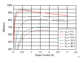
Note:
Figure 12-2 BUCK1 Efficiency | VBUCK1 = 3.3 V |
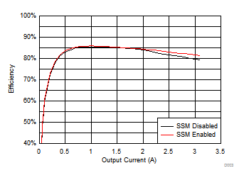
Note:
Figure 12-4 BUCK1 Efficiency| VBUCK1 = 3.3 V | VIN = 13 V |
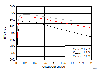
Note:
Figure 12-6 BUCK2 Efficiency| VBUCK1 = 3.3 V | LOUT = IHLP2525CZER1R0M5A | |
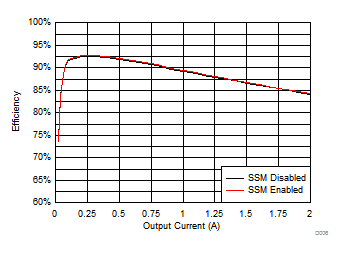
Note:
Figure 12-8 BUCK2 Efficiency| VBUCK1 = 3.3 V | VBUCK2 = 1.8 V | |
| LOUT = IHLP2525CZER1R0M5A | ||
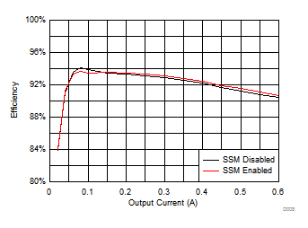
Note:
Figure 12-10 BOOST Efficiency| VBUCK1 = 3.3 V | LOUT = IHLP2525CZER1R5M5A | |

Note:
Figure 12-12 BUCK1 Load and Line
Regulation| VBUCK1 = 3.6 V |
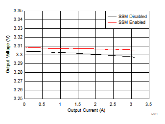
Note:
Figure 12-14 BUCK1 Load Regulation| VBUCK1 = 3.3 V |
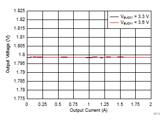
Note:
Figure 12-16 BUCK2 Load Regulation| VBUCK2 = 1.8 V | COUT = 22 µF + 10 µF | |
| LOUT = IHLP2525CZER1R0M5A | ||
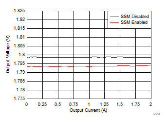
Note:
Figure 12-18 BUCK2 Load Regulation| VBUCK2 = 1.8 V | COUT = 22 µF + 10 µF | |
| VBUCK1 = 3.3 V | LOUT = IHLP2525CZER1R0M5A | |

Note:
Figure 12-20 BOOST Load Regulation| VBUCK1 = 3.3 V | COUT = 22 µF + 10 µF | |
| LOUT = IHLP2525CZER1R5M5A | ||

Note:
Figure 12-22 BUCK1 Load Transient| VOUT (VBUCK1) = 3.6 V | TR = TF = 1 µs | |
| IOUT = 0 A to 2 A |
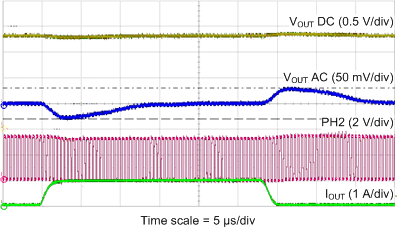
Note:
Figure 12-24 BUCK2 Load Transient| VOUT (VBUCK2) = 1.8 V | TR = TF = 1 µs | |
| VBUCK1 = 3.3 V | IOUT = 0 A to 1 A |
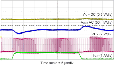
Note:
Figure 12-26 BUCK2 Load Transient| VOUT (VBUCK2) = 1.2 V | TR = TF = 1 µs | |
| VBUCK1 = 3.6 V | IOUT = 0 A to 1 A |
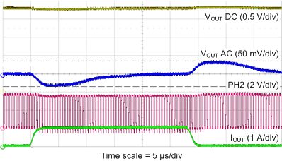
Note:
Figure 12-28 BUCK2 Load Transient| VOUT (VBUCK2) = 2.3 V | TR = TF = 1 µs | |
| VBUCK1 = 3.6 V | IOUT = 0 A to 1 A |
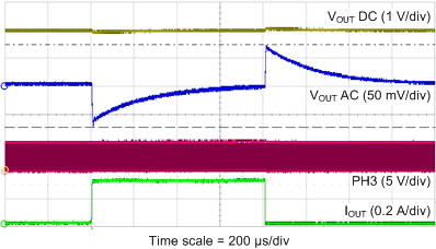
Note:
Figure 12-30 BOOST Load Transient| VOUT (VBOOST) = 5 V | TR = TF = 1 µs | |
| VBUCK1 = 3.6 V | IOUT = 0 A to 0.6 A |
Note:
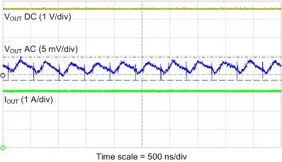
Figure 12-32 BUCK1 Output Voltage Ripple| VOUT (VBUCK1) = 3.6 V | IOUT = 3.1 A |
Note:
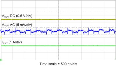
Figure 12-34 BUCK2 Output Voltage Ripple| VOUT (VBUCK2) = 1.2 V | VBUCK1 = 3.3 V | IOUT = 2 A |
Note:
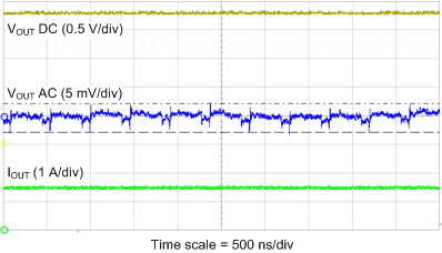
Figure 12-36 BUCK2 Output Voltage Ripple| VOUT (VBUCK2) = 2.3 V | VBUCK1 = 3.3 V | IOUT = 1.5 A |

Note:
Figure 12-38 BUCK2 Output Voltage Ripple| VOUT (VBUCK2) = 1.8 V | SSM Enabled | IOUT = 2 A |
| VBUCK1 = 3.3 V |
Note:
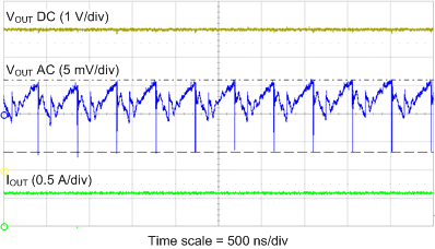
Figure 12-40 BOOST Output Voltage Ripple| VOUT (VBOOST) = 5 V | VBUCK1 = 3.6 V | IOUT = 0.6 A |
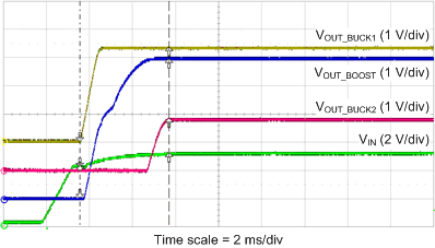
Note:
Figure 12-42 Start-up With VIN and
WAKE Connected Together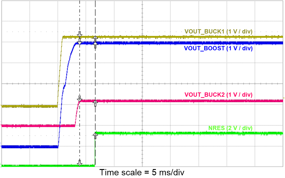
A.
Figure 12-44 Start-up Showing NRES Output With
Short NRES Extension Delay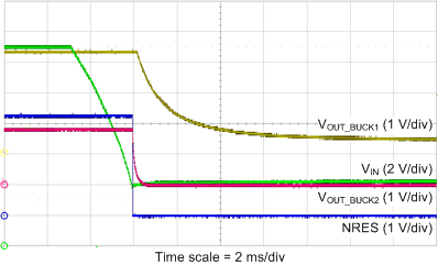 Figure 12-46 Shutdown Showing NRES Output
Note:
Figure 12-3 BUCK1 Efficiency| VBUCK1 = 3.6 V |
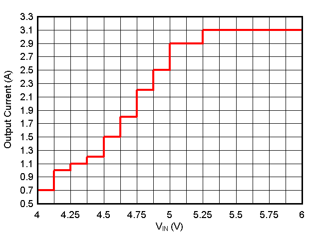
A.
Figure 12-5 BUCK1 Output Current at Low
VIN Conditions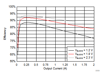
Note:
Figure 12-7 BUCK2 Efficiency| VBUCK1 = 3.6 V | LOUT = IHLP2525CZER1R0M5A | |
Note:
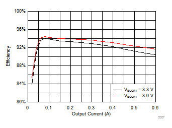
Figure 12-9 BOOST Efficiency| LOUT = IHLP2525CZER1R5M5A |
Note:
Figure 12-11 BUCK1 Load and Line
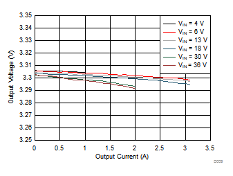
Regulation| VBUCK1 = 3.3 V |
Note:
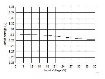
Figure 12-13 BUCK1 Line Regulation| VBUCK1 = 3.3 V | IOUT= 2 A |
Note:
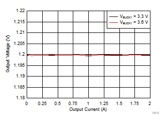
Figure 12-15 BUCK2 Load Regulation| VBUCK2 = 1.2 V | COUT = 22 µF + 10 µF | |
| LOUT = IHLP2525CZER1R0M5A | ||

Note:
Figure 12-17 BUCK2 Load Regulation| VBUCK2 = 2.3 V | COUT = 22 µF + 10 µF | |
| LOUT = IHLP2525CZER1R0M5A | ||
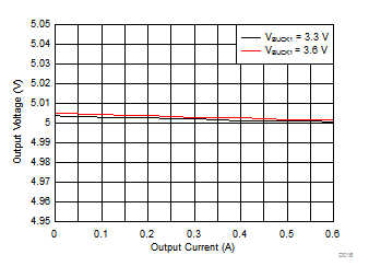
Note:
Figure 12-19 BOOST Load and Line
Regulation| COUT = 22 µF + 10 µF | LOUT = IHLP2525CZER1R5M5A |
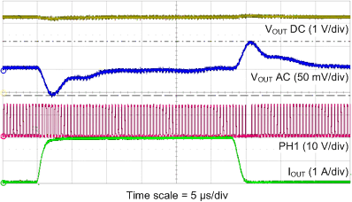
Note:
Figure 12-21 BUCK1 Load Transient| VOUT (VBUCK1) = 3.3 V | TR = TF = 1 µs | |
| IOUT = 0 A to 2 A |
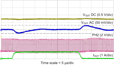
Note:
Figure 12-23 BUCK2 Load Transient| VOUT (VBUCK2) = 1.2 V | TR = TF = 1 µs | |
| VBUCK1 = 3.3 V | IOUT = 0 A to 1 A |
Note:
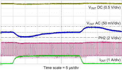
Figure 12-25 BUCK2 Load Transient| VOUT (VBUCK2) = 2.3 V | TR = TF = 1 µs | |
| VBUCK1 = 3.3 V | IOUT = 0 A to 1 A |
Note:
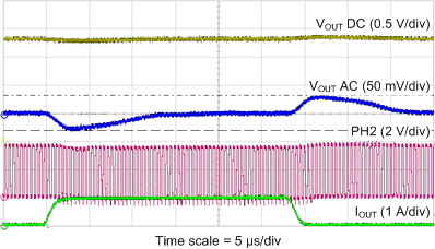
Figure 12-27 BUCK2 Load Transient| VOUT (VBUCK2) = 1.8 V | TR = TF = 1 µs | |
| VBUCK1 = 3.6 V | IOUT = 0 A to 1 A |
Note:
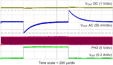
Figure 12-29 BOOST Load Transient| VOUT (VBOOST) = 5 V | TR = TF = 1 µs | |
| VBUCK1 = 3.3 V | IOUT = 0 A to 0.6 A |
Note:
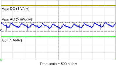
Figure 12-31 BUCK1 Output Voltage Ripple| VOUT (VBUCK1) = 3.3 V | IOUT = 3.1 A |
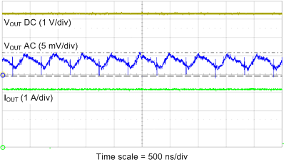
Note:
Figure 12-33 BUCK1 Output Voltage Ripple| VOUT (VBUCK1) = 3.3 V | SSM Enabled | IOUT = 3.1 A |
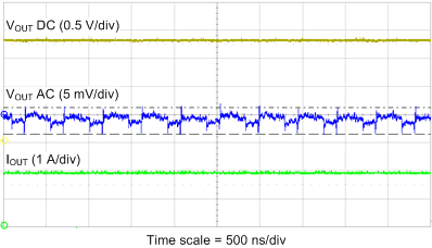
Note:
Figure 12-35 BUCK2 Output Voltage Ripple| VOUT (VBUCK2) = 1.8 V | VBUCK1 = 3.3 V | IOUT = 2 A |

Note:
Figure 12-37 BUCK2 Output Voltage Ripple| VOUT (VBUCK2) = 1.8 V | VBUCK1 = 3.6 V | IOUT = 2 A |
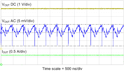
Note:
Figure 12-39 BOOST Output Voltage Ripple| VOUT (VBOOST) = 5 V | VBUCK1 = 3.3 V | IOUT = 0.6 A |
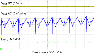
Note:
Figure 12-41 BOOST Output Voltage Ripple| VOUT (VBOOST) = 5 V | SSM Enabled | IOUT = 0.6 A |
| VBUCK1 = 3.3 V |

Note:
Figure 12-43 Start-up Showing NRES Output With
Long NRES Extension Delay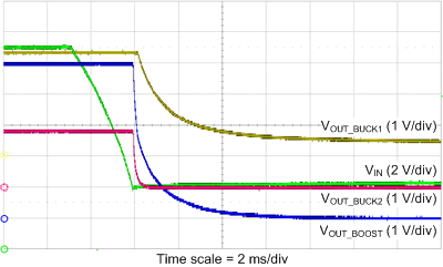
Note:
Figure 12-45 Shutdown With
VIN