ZHCSL05C October 2019 – October 2023 TPS65313-Q1
PRODUCTION DATA
- 1
- 1 特性
- 2 应用
- 3 说明
- 4 器件功能方框图
- 5 Revision History
- 6 说明(续)
- 7 Device Option Table
- 8 Pin Configuration and Functions
-
9 Specifications
- 9.1 Absolute Maximum Ratings
- 9.2 ESD Ratings
- 9.3 Recommended Operating Conditions
- 9.4 Thermal Information
- 9.5 Power-On-Reset, Current Consumption, and State Timeout Characteristics
- 9.6 PLL/Oscillator and SYNC_IN Pin Characteristics
- 9.7 Wide-VIN Synchronous Buck Regulator (Wide-VIN BUCK) Characteristics
- 9.8 Low-Voltage Synchronous Buck Regulator (LV BUCK) Characteristics
- 9.9 Synchronous Boost Converter (BOOST) Characteristics
- 9.10 Internal Voltage Regulator (VREG) Characteristics
- 9.11 Voltage Monitors for Regulators Characteristics
- 9.12 External General Purpose Voltage Monitor Characteristics
- 9.13 VIN and VIN_SAFE Under-Voltage and Over-Voltage Warning Characteristics
- 9.14 WAKE Input Characteristics
- 9.15 NRES (nRESET) Output Characteristics
- 9.16 ENDRV/nIRQ Output Characteristics
- 9.17 Analog DIAG_OUT
- 9.18 Digital INPUT/OUTPUT IOs (SPI Interface IOs, DIAG_OUT/SYNC_OUT, MCU_ERROR)
- 9.19 BUCK1, BUCK2, BOOST Thermal Shutdown / Over Temperature Protection Characteristics
- 9.20 PGNDx Loss Detection Characteristics
- 9.21 SPI Timing Requirements
- 9.22 SPI Characteristics
- 9.23 Typical Characteristics
- 10Parameter Measurement Information
-
11Detailed Description
- 11.1 Overview
- 11.2 Functional Block Diagram
- 11.3
Wide-VIN Buck Regulator (BUCK1)
- 11.3.1 Fixed-Frequency Voltage-Mode Step-Down Regulator
- 11.3.2 Operation
- 11.3.3 Voltage Monitoring (Monitoring and Protection)
- 11.3.4 Overcurrent Protection (Monitoring and Protection)
- 11.3.5 Thermal Warning and Shutdown Protection (Monitoring and Protection)
- 11.3.6 Overvoltage Protection (OVP) (Monitoring and Protection)
- 11.3.7 Extreme Overvoltage Protection (EOVP) (Monitoring and Protection)
- 11.4
Low-Voltage Buck Regulator (BUCK2)
- 11.4.1 Fixed-Frequency Peak-Current Mode Step-Down Regulator
- 11.4.2 Operation
- 11.4.3 Output Voltage Monitoring (Monitoring and Protection)
- 11.4.4 Overcurrent Protection (Monitoring and Protection)
- 11.4.5 Thermal Sensor Warning and Thermal Shutdown Protection (Monitoring and Protection)
- 11.4.6 Overvoltage Protection (OVP) (Monitoring and Protection)
- 11.5 Low-Voltage Boost Converter (BOOST)
- 11.6 VREG Regulator
- 11.7
BUCK1, BUCK2, and BOOST Switching Clocks and Synchronization (SYNC_IN) Clock
- 11.7.1 Internal fSW Clock Configuration (fSW Derived from an Internal Oscillator)
- 11.7.2 BUCK1 Switching Clock-Monitor Error (Internal fSW Clock Configuration)
- 11.7.3 BUCK2 Switching Clock-Monitor Error (Internal fSW Clock Configuration)
- 11.7.4 BOOST Switching Clock-Monitor Error (Internal fSW Clock Configuration)
- 11.7.5 External fSW Clock Configuration (fSW Derived from SYNC_IN and PLL Clocks)
- 11.8 BUCK1, BUCK2, and BOOST Switching-Clock Spread-Spectrum Modulation
- 11.9
Monitoring, Protection and Diagnostics Overview
- 11.9.1 Safety Functions and Diagnostic Overview
- 11.9.2 Supply Voltage Monitor (VMON)
- 11.9.3 Clock Monitors
- 11.9.4 Analog Built-In Self-Test
- 11.9.5 Logic Built-In Self-Test
- 11.9.6 Junction Temperature Monitors
- 11.9.7 Current Limit
- 11.9.8 Loss of Ground (GND)
- 11.9.9 Diagnostic Output Pin (DIAG_OUT)
- 11.9.10 Watchdog
- 11.9.11 MCU Error Signal Monitor
- 11.9.12 NRES Driver
- 11.9.13 ENDRV/nIRQ Driver
- 11.9.14 CRC Protection for the Device Configuration Registers
- 11.9.15 CRC Protection for the Device EEPROM Registers
- 11.10 General-Purpose External Supply Voltage Monitors
- 11.11 Analog Wake-up and Failure Latch
- 11.12 Power-Up and Power-Down Sequences
- 11.13 Device Fail-Safe State Controller (Monitoring and Protection)
- 11.14 Wakeup
- 11.15 Serial Peripheral Interface (SPI)
- 11.16 Register Maps
-
12Applications, Implementation, and Layout
- 12.1 Application Information
- 12.2
Typical Application
- 12.2.1 Design Requirements
- 12.2.2
Detailed Design Procedure
- 12.2.2.1 Selecting the BUCK1, BUCK2, and BOOST Output Voltages
- 12.2.2.2 Selecting the BUCK1, BUCK2, and BOOST Inductors
- 12.2.2.3 Selecting the BUCK1 and BUCK2 Output Capacitors
- 12.2.2.4 Selecting the BOOST Output Capacitors
- 12.2.2.5 Input Filter Capacitor Selection for BUCK1, BUCK2, and BOOST
- 12.2.2.6 Input Filter Capacitors on AVIN and VIN_SAFE Pins
- 12.2.2.7 Bootstrap Capacitor Selection
- 12.2.2.8 Internal Linear Regulator (VREG) Output Capacitor Selection
- 12.2.2.9 EXTSUP Pin
- 12.2.2.10 WAKE Input Pin
- 12.2.2.11 VIO Supply Pin
- 12.2.2.12 External General-Purpose Voltage Monitor Input Pins (EXT_VSENSE1 and EXT_VSENSE2)
- 12.2.2.13 SYNC_IN Pin
- 12.2.2.14 MCU_ERR Pin
- 12.2.2.15 NRES Pin
- 12.2.2.16 ENDRV/nIRQ Pin
- 12.2.2.17 DIAG_OUT Pin
- 12.2.2.18 SPI Pins (NCS,SCK, SDI, SDO)
- 12.2.2.19 PBKGx, AGND, DGND, and PGNDx Pins
- 12.2.2.20 Calculations for Power Dissipation and Junction Temperature
- 12.2.3 Application Curves
- 12.2.4 Layout
- 12.3 Power Supply Coupling and Bulk Capacitors
- 13Device and Documentation Support
- 14Mechanical, Packaging, and Orderable Information
11.9.9 Diagnostic Output Pin (DIAG_OUT)
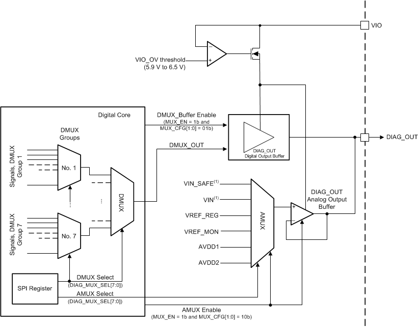
The multiplexer switches internal analog and digital signals to the DIAG_OUT pin. The SPI register DIAG_MUX_SEL sets the mode of this multiplexer. Both the analog and digital signals have separate buffers (AMUX buffer and DMUX buffer) for sufficient drive capability.
The MUX_CFG[1:0] bits in the DIAG_CTRL register selects the type of signal (either analog or digital) on the DIAG_OUT pin. The MUX_EN control bit in the DIAG_CTRL register enables the DIAG_OUT multiplexer output. When disabled, the DIAG_OUT pin is in the high-impedance state.
The VIO pin supplies both the AMUX buffer and DMUX buffer. When an overvoltage event occurs on the VIO pin, the device disconnects the supply to the AMUX and DMUX buffers as shown in Figure 11-14.

- The marked analog signals are connected to the AMUX through a resistor divider.