ZHCSDG2 March   2015 TPS65632

PRODUCTION DATA.  

  1. 特性
  2. 应用范围
  3. 说明
  4. 简化电路原理图
  5. 修订历史记录
  6. Pin Configuration and Functions
  7. Specifications
    1. 7.1 Absolute Maximum Ratings
    2. 7.2 ESD Ratings
    3. 7.3 Recommended Operating Conditions
    4. 7.4 Thermal Information
    5. 7.5 Electrical Characteristics
    6. 7.6 Timing Requirements
    7. 7.7 Typical Characteristics
  8. Detailed Description
    1. 8.1 Overview
    2. 8.2 Functional Block Diagram
    3. 8.3 Feature Description
      1. 8.3.1 Boost Converter 1 (VPOS)
        1. 8.3.1.1 V(POS) Boost Output Sense (FBS Pin)
      2. 8.3.2 Inverting Buck-Boost Converter (VNEG)
        1. 8.3.2.1 Programming VNEG
        2. 8.3.2.2 Controlling VNEG Transition Time
      3. 8.3.3 Boost Converter 2 (AVDD)
      4. 8.3.4 Soft Start and Start-Up Sequence
      5. 8.3.5 Enable (CTRL)
      6. 8.3.6 Undervoltage Lockout
      7. 8.3.7 Short-Circuit Protection
        1. 8.3.7.1 Short Circuits During Operation
        2. 8.3.7.2 Short Circuits During Start Up
      8. 8.3.8 Output Discharge During Shut Down
      9. 8.3.9 Thermal Shutdown
    4. 8.4 Device Functional Modes
      1. 8.4.1 Operation with VI < 2.9 V
      2. 8.4.2 Operation with VI ≈ VPOS (Diode Mode)
      3. 8.4.3 Operation with CTRL
  9. Application and Implementation
    1. 9.1 Application Information
    2. 9.2 Typical Application
      1. 9.2.1 Design Requirements
      2. 9.2.2 Detailed Design Procedure
        1. 9.2.2.1 Inductor Selection
        2. 9.2.2.2 Capacitor Selection
      3. 9.2.3 Application Curves
  10. 10Power Supply Recommendations
  11. 11Layout
    1. 11.1 Layout Guidelines
    2. 11.2 Layout Example
  12. 12器件和文档支持
    1. 12.1 器件支持
      1. 12.1.1 第三方米6体育平台手机版_好二三四免责声明
    2. 12.2 商标
    3. 12.3 静电放电警告
    4. 12.4 术语表
  13. 13机械、封装和可订购信息

封装选项

机械数据 (封装 | 引脚)
散热焊盘机械数据 (封装 | 引脚)
订购信息

11 Layout

11.1 Layout Guidelines

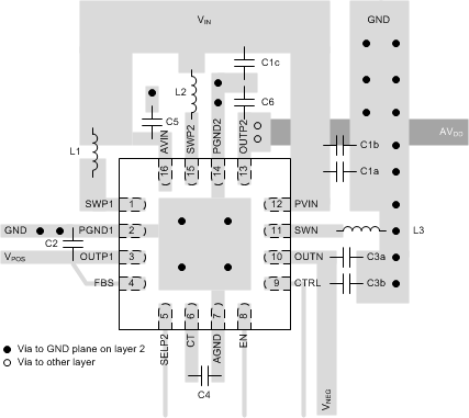
  • Place the input capacitor on PVIN and the output capacitor on OUTN as close as possible to device. Use short and wide traces to connect the input capacitor on PVIN and the output capacitor on OUTN.
  • Place the output capacitor on OUTP1 and OUTP2 as close as possible to device. Use short and wide traces to connect the output capacitor on OUTP1 and OUTP2.
  • Connect the ground of CT capacitor with AGND, pin 7, directly.
  • Connect input ground and output ground on the same board layer, not through via hole.
  • Connect AGND, PGND1 and PGND2 with exposed thermal pad.

11.2 Layout Example
TPS65632 layout_slvscy2.gifFigure 32. Recommended PCB Layout