ZHCSEF7G December 2014 – February 2019 TPS659037
PRODUCTION DATA.
- 1 器件概述
- 2 修订历史记录
- 3 Pin Configuration and Functions
-
4 Specifications
- 4.1 Absolute Maximum Ratings
- 4.2 ESD Ratings
- 4.3 Recommended Operating Conditions
- 4.4 Thermal Information
- 4.5 Electrical Characteristics: Latch Up Rating
- 4.6 Electrical Characteristics: LDO Regulator
- 4.7 Electrical Characteristics: Dual-Phase (SMPS12 and SMPS45) and Triple-Phase (SMPS123 and SMPS457) Regulators
- 4.8 Electrical Characteristics: Stand-Alone Regulators (SMPS3, SMPS6, SMPS7, SMPS8, and SMPS9)
- 4.9 Electrical Characteristics: Reference Generator (Bandgap)
- 4.10 Electrical Characteristics: 16-MHz Crystal Oscillator, 32-kHz RC Oscillator, and Output Buffers
- 4.11 Electrical Characteristics: DC-DC Clock Sync
- 4.12 Electrical Characteristics: 12-Bit Sigma-Delta ADC
- 4.13 Electrical Characteristics: Thermal Monitoring and Shutdown
- 4.14 Electrical Characteristics: System Control Threshold
- 4.15 Electrical Characteristics: Current Consumption
- 4.16 Electrical Characteristics: Digital Input Signal Parameters
- 4.17 Electrical Characteristics: Digital Output Signal Parameters
- 4.18 Electrical Characteristics: I/O Pullup and Pulldown
- 4.19 I2C Interface Timing Requirements
- 4.20 SPI Timing Requirements
- 4.21 Typical Characteristics
-
5 Detailed Description
- 5.1 Overview
- 5.2 Functional Block Diagram
- 5.3
Feature Description
- 5.3.1 Power Management
- 5.3.2
Power Resources (Step-Down and Step-Up SMPS Regulators, LDOs)
- 5.3.2.1
Step-Down Regulators
- 5.3.2.1.1 Sync Clock Functionality
- 5.3.2.1.2 Output Voltage and Mode Selection
- 5.3.2.1.3 Current Monitoring and Short Circuit Detection
- 5.3.2.1.4 POWERGOOD
- 5.3.2.1.5 DVS-Capable Regulators
- 5.3.2.1.6 Non DVS-Capable Regulators
- 5.3.2.1.7 Step-Down Converters SMPS12 and SMPS123
- 5.3.2.1.8 Step-Down Converter SMPS45 and SMPS457
- 5.3.2.1.9 Step-Down Converters SMPS3, SMPS6, SMPS7, SMPS8, and SMPS9
- 5.3.2.2 LDOs – Low Dropout Regulators
- 5.3.2.1
Step-Down Regulators
- 5.3.3 Long-Press Key Detection
- 5.3.4 RTC
- 5.3.5 GPADC – 12-Bit Sigma-Delta ADC
- 5.3.6 General-Purpose I/Os (GPIO Pins)
- 5.3.7 Thermal Monitoring
- 5.3.8 Interrupts
- 5.3.9 Control Interfaces
- 5.3.10 Device Identification
- 5.4 Device Functional Modes
-
6 Application and Implementation
- 6.1 Application Information
- 6.2
Typical Application
- 6.2.1 Design Requirements
- 6.2.2 Detailed Design Procedure
- 6.2.3 Application Curves
- 7 Power Supply Recommendations
- 8 Layout
- 9 器件和文档支持
- 10机械、封装和可订购信息
5.3.2.1.5 DVS-Capable Regulators
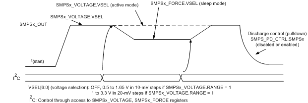
The step-down converters SMPS12 or SMPS123, SMPS45 or SMPS457, SMPS6, and SMPS8 are DVS-capable and have some additional parameters for control. The slew rate of the output voltage during a change in the voltage level is fixed at 2.5 mV/μs. The control for the two different voltage levels (ROOF and FLOOR) with the NSLEEP and ENABLE1 signals is available. The control bits for the output voltage slew rate control the following additional control bits. When the ROOF_FLOOR control is not used, two different voltage levels can be selected with the CMD bit in the SMPSx_FORCE register.
- The output voltage slew rate for achieving new output voltage value is fixed at 2.5 mV/μs.
- The NSLEEP and ENABLE1 pins can be used for roof-floor control of SMPS. For roof-floor operation sets the SMPSx_CTRL.ROOF_FLOOR_EN register, and assign SMPS to NSLEEP and ENABLE1 in the NSLEEP_SMPS_ASSIGN and ENABLE1_SMPS_ASSIGN registers. When the controlling pin is active, the SMPS output value is defined by the SMPSx_VOLTAGE register. When the controlling pin is not active, the SMPS output value is defined by the SMPSx_FORCE register.
- Set the second value for the output voltage with the SMPSx_FORCE.VSEL register. A value of 0x0 disables the SMPS (OFF).
- Select which register, SMPSx_VOLTAGE or SMPSx_FORCE, to use with the SMPSx_FORCE.CMD bit. The default is the voltage setting of SMPSx_VOLTAGE. For the CMD bit to work, ensure that SMPSx_CTRL.ROOF_FLOOR_EN = 0.
Figure 5-5 and Figure 5-4 show the SMPS controls for DVS.
 Figure 5-4 DVS - SMPS Controls
Voltage Control Through I2C (SMPSx_CTRL.ROOF_FLOOR_EN = 0)

1. See Table 5-13.
Figure 5-5 DVS - SMPS Controls
Voltage Control Through External Pin (SMPSx_CTRL.ROOF_FLOOR_EN = 1)