ZHCSEF7G December 2014 – February 2019
PRODUCTION DATA.
- 1 器件概述
- 2 修订历史记录
- 3 Pin Configuration and Functions
-
4 Specifications
- 4.1 Absolute Maximum Ratings
- 4.2 ESD Ratings
- 4.3 Recommended Operating Conditions
- 4.4 Thermal Information
- 4.5 Electrical Characteristics: Latch Up Rating
- 4.6 Electrical Characteristics: LDO Regulator
- 4.7 Electrical Characteristics: Dual-Phase (SMPS12 and SMPS45) and Triple-Phase (SMPS123 and SMPS457) Regulators
- 4.8 Electrical Characteristics: Stand-Alone Regulators (SMPS3, SMPS6, SMPS7, SMPS8, and SMPS9)
- 4.9 Electrical Characteristics: Reference Generator (Bandgap)
- 4.10 Electrical Characteristics: 16-MHz Crystal Oscillator, 32-kHz RC Oscillator, and Output Buffers
- 4.11 Electrical Characteristics: DC-DC Clock Sync
- 4.12 Electrical Characteristics: 12-Bit Sigma-Delta ADC
- 4.13 Electrical Characteristics: Thermal Monitoring and Shutdown
- 4.14 Electrical Characteristics: System Control Threshold
- 4.15 Electrical Characteristics: Current Consumption
- 4.16 Electrical Characteristics: Digital Input Signal Parameters
- 4.17 Electrical Characteristics: Digital Output Signal Parameters
- 4.18 Electrical Characteristics: I/O Pullup and Pulldown
- 4.19 I2C Interface Timing Requirements
- 4.20 SPI Timing Requirements
- 4.21 Typical Characteristics
-
5 Detailed Description
- 5.1 Overview
- 5.2 Functional Block Diagram
- 5.3
Feature Description
- 5.3.1 Power Management
- 5.3.2
Power Resources (Step-Down and Step-Up SMPS Regulators, LDOs)
- 5.3.2.1
Step-Down Regulators
- 5.3.2.1.1 Sync Clock Functionality
- 5.3.2.1.2 Output Voltage and Mode Selection
- 5.3.2.1.3 Current Monitoring and Short Circuit Detection
- 5.3.2.1.4 POWERGOOD
- 5.3.2.1.5 DVS-Capable Regulators
- 5.3.2.1.6 Non DVS-Capable Regulators
- 5.3.2.1.7 Step-Down Converters SMPS12 and SMPS123
- 5.3.2.1.8 Step-Down Converter SMPS45 and SMPS457
- 5.3.2.1.9 Step-Down Converters SMPS3, SMPS6, SMPS7, SMPS8, and SMPS9
- 5.3.2.2 LDOs – Low Dropout Regulators
- 5.3.2.1
Step-Down Regulators
- 5.3.3 Long-Press Key Detection
- 5.3.4 RTC
- 5.3.5 GPADC – 12-Bit Sigma-Delta ADC
- 5.3.6 General-Purpose I/Os (GPIO Pins)
- 5.3.7 Thermal Monitoring
- 5.3.8 Interrupts
- 5.3.9 Control Interfaces
- 5.3.10 Device Identification
- 5.4 Device Functional Modes
-
6 Application and Implementation
- 6.1 Application Information
- 6.2
Typical Application
- 6.2.1 Design Requirements
- 6.2.2 Detailed Design Procedure
- 6.2.3 Application Curves
- 7 Power Supply Recommendations
- 8 Layout
- 9 器件和文档支持
- 10机械、封装和可订购信息
5.3.5 GPADC – 12-Bit Sigma-Delta ADC
The GPADC consists of a 12-bit sigma-delta ADC combined with an analog input multiplexer. The GPADC allows the host processor to monitor a variety of analog signals using analog-to-digital conversion on the input source. After the conversion completes, an interrupt is generated for the host processor and it can read the result of the conversion through the I2C interface.
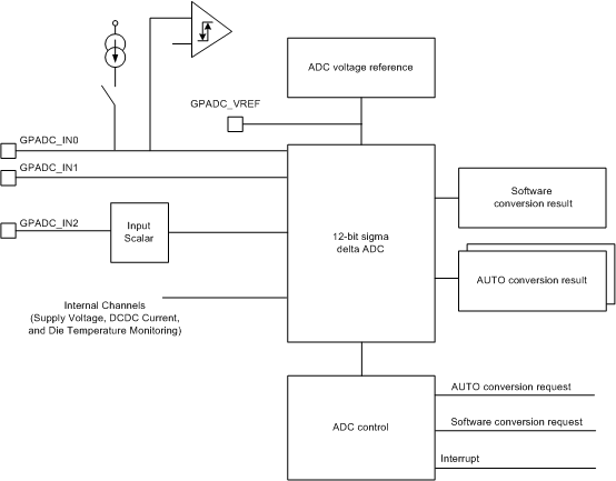
The GPADC on this PMIC supports 16 analog inputs. However only a total of 9 inputs are available for the application use. Three of these inputs are available on external pins, and the remaining six are dedicated to internal resource monitoring. One of the three external inputs is associated with a current source allowing measurements of resistive elements (thermal sensor). To improve the measurement accuracy, the reference voltages GPADC_VREF can be used with an external resistor for the NTC resistor measurement. The reference voltage GPADC_VREF is always present when the GPADC is enabled.
GPADC_IN0 is associated with three selectable current sources. The selectable current levels are 5, 15, and 20 μA.
GPADC_IN1 is intended to measure temperature with an NTC sensor connected to ground. Two resistors, one in parallel with the NTC resistor and the other one between GPADC_IN1 and GPADC_VREF, can be used to modify the exponential function of the NTC resistor.
Figure 5-9 shows the block diagram of the GPADC.
 Figure 5-9 Block Diagram of the GPADC
 For all the measurements performed by the monitoring GPADC, voltage dividers, current to voltage converters, and current source are integrated in the TPS659037 device to scale the signal to be measured to the GPADC input range.
The conversion requests are initiated by the host processor either by software through the I2C. This mode is useful when real-time conversion is required.
Two kinds of conversion requests are available with the following priority:
- Asynchronous conversion request (SW)
- Periodic conversion (AUTO)
The EXTEND_DELAY bit in the GPADC_RT_CTRL register can extend by 400 μs the delay from the channel selection or triggering to the sampling.
Use Equation 4 to convert from the GPADC code to the internal die temperature using GPADC channels 12 and 13.

Table 5-3 GPADC Channel Assignments
| CHANNEL | TYPE | INPUT VOLTAGE FULL RANGE(1) | INPUT VOLTAGE PERFORMANCE RANGE(2) | SCALER | OPERATION |
|---|---|---|---|---|---|
| 0 (GPADC_IN0) | External(3) | 0 to 1.25 V | 0.01 to 1.215 V | No | Resistor value or general purpose. Select source current 0, 5, 15, or 20 μA |
| 1 (GPADC_IN1) | External(3) | 0 to 1.25 V | 0.01 to 1.215 V | No | Platform temperature, NTC resistor value and general purpose |
| 2 (GPADC_IN2) | External(3) | 0 to 2.5 V | 0.02 to 2.43 V | 2 | Audio accessory or general purpose |
| 7 (VCC_SENSE) | Internal | 2.5 to 5 V when HIGH_VCC_SENSE = 0
2.3 V to (VCC1–1 V) when HIGH_VCC_SENSE = 1 |
2.5 to 4.86 V when HIGH_VCC_SENSE = 0
2.3 V to (VCC1–1 V) when HIGH_VCC_SENSE = 1 |
4 | System supply voltage (VCC_SENSE) |
| 10 (VBUS) | Internal | 0 to 6.875V | 0.055 to 5.25 V | 5.5 | VBUS Voltage |
| 11 | Internal | 0 to 1.25 V | No | DC-DC current probe | |
| 12 | Internal | 0 to 1.25 V | 0 to 1.215 V | No | PMIC internal die temperature |
| 13 | Internal | 0 to 1.25 V | 0 to 1.215 V | No | PMIC internal die temperature |
| 15 | Internal | 0 to VCC1 V | 0.055 to VCC1 V | 5 | Test network |