ZHCSEF7G December 2014 – February 2019 TPS659037
PRODUCTION DATA.
- 1 器件概述
- 2 修订历史记录
- 3 Pin Configuration and Functions
-
4 Specifications
- 4.1 Absolute Maximum Ratings
- 4.2 ESD Ratings
- 4.3 Recommended Operating Conditions
- 4.4 Thermal Information
- 4.5 Electrical Characteristics: Latch Up Rating
- 4.6 Electrical Characteristics: LDO Regulator
- 4.7 Electrical Characteristics: Dual-Phase (SMPS12 and SMPS45) and Triple-Phase (SMPS123 and SMPS457) Regulators
- 4.8 Electrical Characteristics: Stand-Alone Regulators (SMPS3, SMPS6, SMPS7, SMPS8, and SMPS9)
- 4.9 Electrical Characteristics: Reference Generator (Bandgap)
- 4.10 Electrical Characteristics: 16-MHz Crystal Oscillator, 32-kHz RC Oscillator, and Output Buffers
- 4.11 Electrical Characteristics: DC-DC Clock Sync
- 4.12 Electrical Characteristics: 12-Bit Sigma-Delta ADC
- 4.13 Electrical Characteristics: Thermal Monitoring and Shutdown
- 4.14 Electrical Characteristics: System Control Threshold
- 4.15 Electrical Characteristics: Current Consumption
- 4.16 Electrical Characteristics: Digital Input Signal Parameters
- 4.17 Electrical Characteristics: Digital Output Signal Parameters
- 4.18 Electrical Characteristics: I/O Pullup and Pulldown
- 4.19 I2C Interface Timing Requirements
- 4.20 SPI Timing Requirements
- 4.21 Typical Characteristics
-
5 Detailed Description
- 5.1 Overview
- 5.2 Functional Block Diagram
- 5.3
Feature Description
- 5.3.1 Power Management
- 5.3.2
Power Resources (Step-Down and Step-Up SMPS Regulators, LDOs)
- 5.3.2.1
Step-Down Regulators
- 5.3.2.1.1 Sync Clock Functionality
- 5.3.2.1.2 Output Voltage and Mode Selection
- 5.3.2.1.3 Current Monitoring and Short Circuit Detection
- 5.3.2.1.4 POWERGOOD
- 5.3.2.1.5 DVS-Capable Regulators
- 5.3.2.1.6 Non DVS-Capable Regulators
- 5.3.2.1.7 Step-Down Converters SMPS12 and SMPS123
- 5.3.2.1.8 Step-Down Converter SMPS45 and SMPS457
- 5.3.2.1.9 Step-Down Converters SMPS3, SMPS6, SMPS7, SMPS8, and SMPS9
- 5.3.2.2 LDOs – Low Dropout Regulators
- 5.3.2.1
Step-Down Regulators
- 5.3.3 Long-Press Key Detection
- 5.3.4 RTC
- 5.3.5 GPADC – 12-Bit Sigma-Delta ADC
- 5.3.6 General-Purpose I/Os (GPIO Pins)
- 5.3.7 Thermal Monitoring
- 5.3.8 Interrupts
- 5.3.9 Control Interfaces
- 5.3.10 Device Identification
- 5.4 Device Functional Modes
-
6 Application and Implementation
- 6.1 Application Information
- 6.2
Typical Application
- 6.2.1 Design Requirements
- 6.2.2 Detailed Design Procedure
- 6.2.3 Application Curves
- 7 Power Supply Recommendations
- 8 Layout
- 9 器件和文档支持
- 10机械、封装和可订购信息
5.4.7 Reset Levels
The TPS659037 device resource control registers are defined by three categories:
- POR registers
- HW (HARDWARE) registers
- SWO (SWITCHOFF) registers
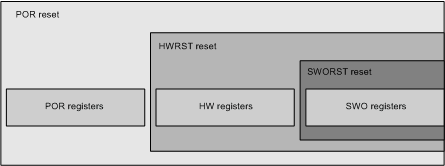
These registers are associated to three levels of reset as described below:
- Power-on reset (POR)
- Power-on reset happens when the TPS659037 device gets its supplies and transition from the NOSUPPLY state to the BACKUP state. This is the global device reset.
- Additionally, SMPS_THERMAL_STATUS, SMPS_SHORT_STATUS,
SMPS_POWERGOOD_MASK, LDO_SHORT_STATUS and SWOFF_STATUS registers are in POR domain. This list is indicative only.
- HWRST – Hardware reset
- Hardware reset happens when any OFF request is configured to generate a hardware reset. This reset triggers a transition to the OFF state from either the ACTIVE or SLEEP state (execute either the ACT2OFF or SLP2OFF sequence).
- SWORST – Switch-off reset
- Switch-off reset happens when any OFF request is configured to not generate a hardware reset. This reset acts as the HWRST, except only the SWO registers are reset. The device goes in the OFF state, from either ACTIVE or SLEEP, and therefore executes the ACT2OFF or SLP2OFF sequence.
- Power resource control registers for SMPS and LDO voltage levels and operating mode control are in SWORST domain. Additionally some registers control the 32-kHz, REGENx and SYSENx, watchdog, external charger control, and VSYS_MON comparator. This list is indicative only.
Table 5-15 lists the reset levels, and Figure 5-25 shows the reset levels versus registers.
Table 5-15 Reset Levels
| LEVEL | RESET TAG | REGISTERS AFFECTED | COMMENT |
|---|---|---|---|
| 0 | POR | POR, HW, SWO | This reset level is the lowest level, for which all registers are reset. |
| 1 | HWRST | HW, SWO | During hardware reset (HWRST), all registers are reset except the POR registers. |
| 2 | SWORST | SWO | Only the SWO registers are reset. |
 Figure 5-25 Reset Levels versus Registers