ZHCSG94L August 2013 – February 2019 TPS659038-Q1 , TPS659039-Q1
PRODUCTION DATA.
- 1 器件概要
- 2 修订历史记录
- 3 Device Comparison
- 4 Pin Configuration and Functions
-
5 Specifications
- 5.1 Absolute Maximum Ratings
- 5.2 ESD Ratings
- 5.3 Recommended Operating Conditions
- 5.4 Thermal Information
- 5.5 Electrical Characteristics: Latch Up Rating
- 5.6 Electrical Characteristics: LDO Regulator
- 5.7 Electrical Characteristics: Dual-Phase (SMPS12 and SMPS45) and Triple-Phase (SMPS123 and SMPS457) Regulators
- 5.8 Electrical Characteristics: Stand-Alone Regulators (SMPS3, SMPS6, SMPS7, SMPS8, and SMPS9)
- 5.9 Electrical Characteristics: Reference Generator (Bandgap)
- 5.10 Electrical Characteristics: 16-MHz Crystal Oscillator, 32-kHz RC Oscillator, and Output Buffers
- 5.11 Electrical Characteristics: DC-DC Clock Sync
- 5.12 Electrical Characteristics: 12-Bit Sigma-Delta ADC
- 5.13 Electrical Characteristics: Thermal Monitoring and Shutdown
- 5.14 Electrical Characteristics: System Control Thresholds
- 5.15 Electrical Characteristics: Current Consumption
- 5.16 Electrical Characteristics: Digital Input Signal Parameters
- 5.17 Electrical Characteristics: Digital Output Signal Parameters
- 5.18 Electrical Characteristics: I/O Pullup and Pulldown Resistance
- 5.19 I2C Interface Timing Requirements
- 5.20 SPI Timing Requirements
- 5.21 Typical Characteristics
-
6 Detailed Description
- 6.1 Overview
- 6.2 Functional Block Diagrams
- 6.3
Feature Description
- 6.3.1 Power Management
- 6.3.2
Power Resources (Step-Down and Step-Up SMPS Regulators, LDOs)
- 6.3.2.1
Step-Down Regulators
- 6.3.2.1.1 Sync Clock Functionality
- 6.3.2.1.2 Output Voltage and Mode Selection
- 6.3.2.1.3 Current Monitoring and Short Circuit Detection
- 6.3.2.1.4 POWERGOOD
- 6.3.2.1.5 DVS-Capable Regulators
- 6.3.2.1.6 Non DVS-Capable Regulators
- 6.3.2.1.7 Step-Down Converters SMPS12 and SMPS123
- 6.3.2.1.8 Step-Down Converter SMPS45 and SMPS457
- 6.3.2.1.9 Step-Down Converters SMPS3, SMPS6, SMPS7, SMPS8, and SMPS9
- 6.3.2.2 LDOs – Low Dropout Regulators
- 6.3.2.1
Step-Down Regulators
- 6.3.3 Long-Press Key Detection
- 6.3.4 RTC
- 6.3.5 GPADC – 12-Bit Sigma-Delta ADC
- 6.3.6 General-Purpose I/Os (GPIO Terminals)
- 6.3.7 Thermal Monitoring
- 6.3.8 Interrupts
- 6.3.9 Control Interfaces
- 6.3.10 Device Identification
- 6.4 Device Functional Modes
-
7 Application and Implementation
- 7.1 Application Information
- 7.2
Typical Application
- 7.2.1 Design Requirements
- 7.2.2 Detailed Design Procedure
- 7.2.3 Application Curves
- 8 Power Supply Recommendations
- 9 Layout
- 10器件和文档支持
- 11机械、封装和可订购信息
6.4.11 System Voltage Monitoring
The power state-machine of the devices are controlled by comparators monitoring the voltage on the VCC_SENSE and VCC1 terminals. For electrical parameters see Section 5.14.
- POR: When the supply at the VCC1 terminal is below the POR threshold, the devices are in the NO SUPPLY state. All functionality, including RTC, is off. When the voltage in VCC1 rises above the POR threshold, the device enters from the NO SUPPLY to the BACKUP state.
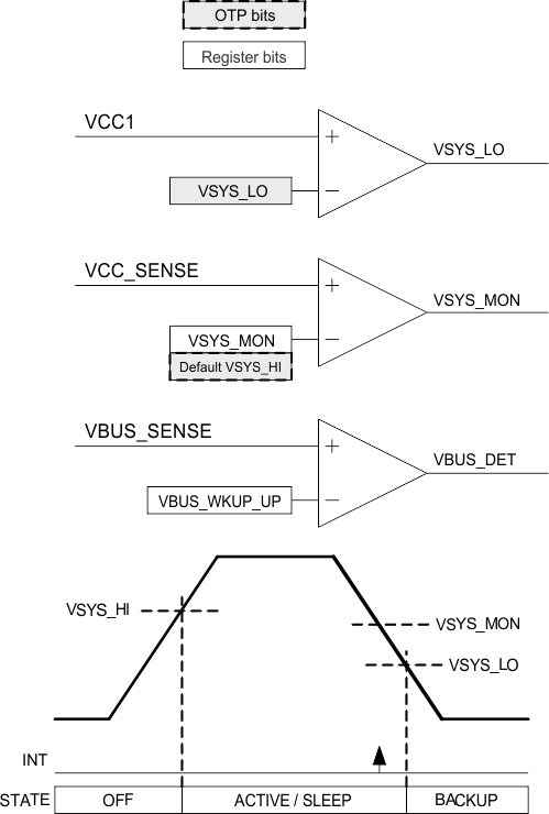
- VSYS_LO: When the voltage on VCC1 terminal rises above VSYS_LO, the device enters from the BACKUP state to the OFF state. When the device is in the ACTIVE, SLEEP, or OFF state and the voltage on VCC1 decreases below VSYS_LO, the device enters BACKUP state. When the device transitions from the ACTIVE state to the BACKUP state, all active SMPS and LDO regulators, except LDOVRTC, are disabled simultaneously. When operating with a 16.384-MHz crystal, the regulators are immediately disabled after VCC1 becomes less than VSYS_LO. When operating without a crystal, a 180-µs deglitch time occurs after VCC1 becomes less than VSYS_LO and before the regulators are disabled. The VSYS_LO level is OTP programmable.
NOTE
For silicon revision 1.3 or earlier, when operating without a crystal, transitioning from the ACTIVE state to the BACKUP state using VSYS_LO while the outputs are active must always be followed by a POR event to make sure the device is reset properly. See Section 6.3.10 to identify the silicon version in the device.
- VSYS_MON: During power up, the VSYS_HI OTP value is used as a threshold for the VSYS_MON comparator which is gating the PMIC start-up (as a threshold for transition from OFF to ACTIVE state). The VSYS_MON comparator monitors the VCC_SENSE terminal. After power up, software can configure the comparator threshold in the VSYS_MON register.
Figure 6-27 shows a block diagram of the system comparators.
 Figure 6-27 System Comparators
 To use comparators in the system:
- The VSYS_LO and VSYS_HI thresholds are defined in the OTP. Software cannot change these levels.
- After start-up, the VSYS_MON comparator is automatically disabled. Software can select a new threshold level using the VSYS_MON register and enable the comparator.
- In order for the same coding on the rising and falling edge, the VSYS_MON comparator does not include hysteresis and therefore can generate multiple interrupts when the voltage level is at the threshold level. New interrupt generation has a 125-μs debounce time which allows the software to mask the interrupt and update the threshold level or disable the comparator before receiving a new interrupt.
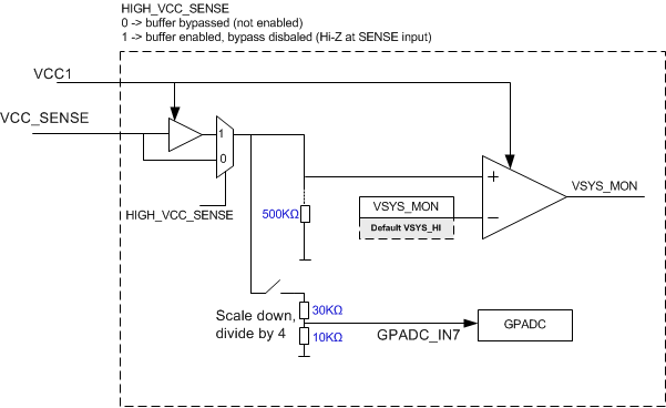
Figure 6-28 shows additional details on the VSYS_MON comparator. When the VSYS_MON comparator is enabled, and the internal buffer is bypassed, input impedance at the VCC_SENSE terminal is 500 kΩ (typical). When the comparators are disabled, the VCC_SENSE terminal is at high impedance mode. If GPADC is enabled to measure channel 6 or channel 7, 40 kΩ is added in parallel to the corresponding comparator. See Table 6-3 for the GPADC input range.
To enable system voltage sensing above 5.25 V, an external resistive divider can be used. Internal buffers are enabled by setting OTP bit HIGH_VCC_SENSE = 1 to provide high impedance for the external resistive dividers. The maximum input level for the internal buffer is VCC1 – 1 V.
 Figure 6-28 VSYS_MON Comparator Details